In the previous post I talked about the quirks and weirdness of ECL gates, Now it’s time to design some more logic with it.
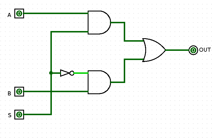
With ECL it is easy to make a NOR/OR gate or D latch, making an AND/NAND gate is a lot more difficult, and usually those are made up from a few NOR/OR gates. This makes logic design a bit interesting, as everything has to be made using NOR/OR gates. As an added bonus, all signals are differential and all gates have an differential output. As an example, the classic 2 input MUX is usually designed like this:
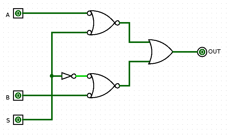
Now lets turn it into an ECL version, using as few gates as possible. The first thing to know is that every AND can be turned into an OR with an inverter added to all in and outputs. Vice versa, an OR can be turned into an AND with inverters at all in and outputs. Optimizing designs like this is called bubble pushing, as it adds inverters, which are indicated by a circle, or bubble, on all in/outputs. So let’s get rid of the ANDs first.
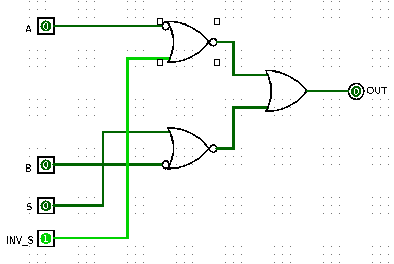
Time to get rid of as many inverters, or bubbles, as possible. First of all, the NOT gate and bubble on the input it’s going to is unnecessary and can be removed. As ECL has differential signals, there also is an inverted version of S available, removing the bubble on the top NOR. The schematic now looks like this:
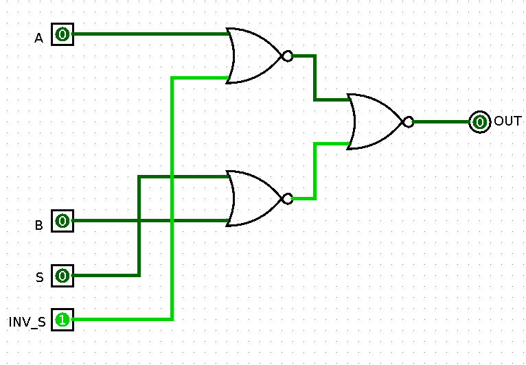
Just 2 bubbles left on the inputs for A and B. Luckily, these are also easy to solve. Removing both the bubbles would invert the output of each NOR, in term inverting the output of the MUX. But with ECL, every gate has an inverted output anyways, solving the problem. The final schematic looks like this:
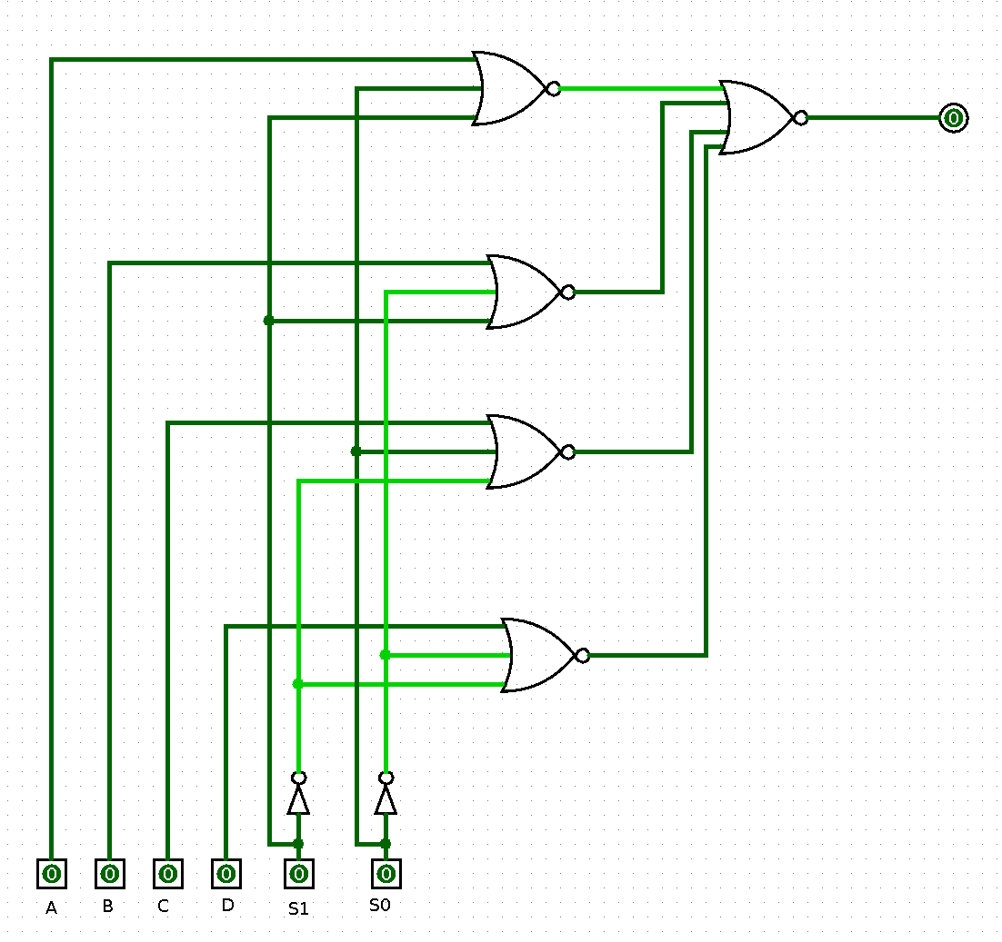
There we go, an NOR based inverter, using just 3 gates, assuming a differential signal is used for the S input. For completion, a 4 input MUX would like like this:
A D FLIP-FLOP
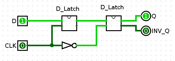
Well, that’s a MUX solved, but flip-flops are also very handy. Luckily turning an D latch into a D flip-flop is simple, just use two and an inverter, or with ECL latches, turn the differential clock signal around.


So, what do you think ?