
a.k.a. the most energy inefficient memory possible.
A computer needs RAM to function, the StupidCPU is no different.
I decided to design the RAM first as it’s a relative straitforward element and the first board also means designing an interface to hookup multiple boars together.
And multiple boards it will be. The design idea is to make everything on 10*10cm PCB’s as those are the cheapest to order from China and one single boards means more things to go wrong.
A backplane like structure will be used with multiple boards plugging in to the backplane to form a computer.
This blog post will discribe the backplane interface and the first board, the RAM board.
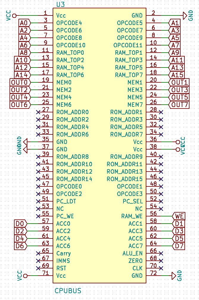
The bus interface:
I wanted something cheap, easy to get and with a lot of IO, 64 to be precise. After a quick look, a simple 2*36 pin pinheader fits the bill perfectly.
With 72 pins, there would be plenty of IO, even with 64 IOs there would still be 8 pins left for power. A 2*36 pinheader is a bit over 9cm wide, meaning that it fits in 10cm easily.
The reason for all this IO is that with fairly small 10*10cm boards there will be a lot of boards, meaning the RAM, ROM, some control and register signals all have to go over the bus.
The bus looks as this at the moment:
– opcode, 12 bits. The lower 8 also make the lower 8 bit RAM address or IMM for the ALU_EN
– RAM_TOP, the 8 upper bits for the RAM address
– ACC, the output from the ALU register
– MEM, the output from the RAM
– ROM_ADDR, the 16 bit address for the ROM
– ALU_EN, control signal to enable the ALU
– Carry, control signal from the ALU that there is a carry bit
– Zero, control signal from the ALU that the output is zero
– IMMS, control signal to the ALU that it needs to use the IMM and not MEM for the calculation
– RAM_WE, control signal that the RAM must write a value to RAM
– PC_JMP, control signal that the program counter must perform a jump
– PC_LDT, control signal that the program counter must load 8 bits for the top 8 bits of the ROM_ADDR
– PC_SEL, control signal that the program counter something RAM? (check)
– Reset, resets the PC and such
– Clock, to clock the CPU
This makes 62 IO in total (check) leaving 2 reserved IO’s from the 64.
In case of the RAM board, the following signals are used:
– Opcode, the lower 8 bits make the lower 8 address bits.
– RAM_TOP, this is the higher 8 bits of the RAM address bits.
– ACC, the data to store
– Mem, the output of the RAM
– RAM_WE, write enable of the RAM
The RAM board:
The RAM board holds a maximum of 128 bytes of RAM. Yes, bytes, not kilobytes or megabytes. Bytes.
To store these, 16 7489 IC’s are used, the 7489 is an old (1970s) 64 bit RAM IC that holds 16 4-bit words. Combine 16 of them and you get 128 bytes of RAM.
You also get one of the most inefficient types of RAM, each 7489 consumes 400mW, always. That makes for a total of 6.4W for 128 bytes of RAM.
In comparison, a modern PC has 8 or more GBs of ram. If this would be scaled to 8GB the power consumption would be immense, over 50 MegaWatt!
The RAM board also has some control logic, though the 7489 chips used take away most of the work.
The 7489 has 2 control signals. WE, to select whether data is read or written to RAM and the ME line, which enables the IC.
When the IC is disabled, the outputs are high.
The 7489 IC is an open drain output device. This means that if the output pins of multiple devices are connected to eachother, one IC pulling one output low makes the output low, even with all other ICs pulling the output high.
Because of this, it is possible to connect the outputs of multiple ICs in parallel and use the ME line to select one device.
An open drain bus is common for busses with multiple devices, for example, the I2C bus works the same way.
the addressing of the RAM is as follows:
The 7489s are arranged into 8 pairs, each pair forming an 8 bit by 16 word RAM block.
The lowest 4 bits go directly to each 7489 RAM IC, an 74×138 decodes the bits 5 to 7 into 8 signals that go to the ME lines of each 7489 pair.
the other 9 addresses go to a 74×260, an dual 5 input NOR gate. THe outputs of this nor gate go back to the 74×138 to disable it, so that if more RAM is added later on there are no incompactibilities.
As the 7489s output is inverted, 2 74×04 NOT gate ICs are needed to invert it again. An array of pull-up resistors is also added as the 7489 outputs are open drain.
The schematic looks like this:

Also visible in the schematic are 16 LEDs. Every board will have these to indicate status, help with debugging and for a cool blinkenlight effect.
The finished PCB looks like this:
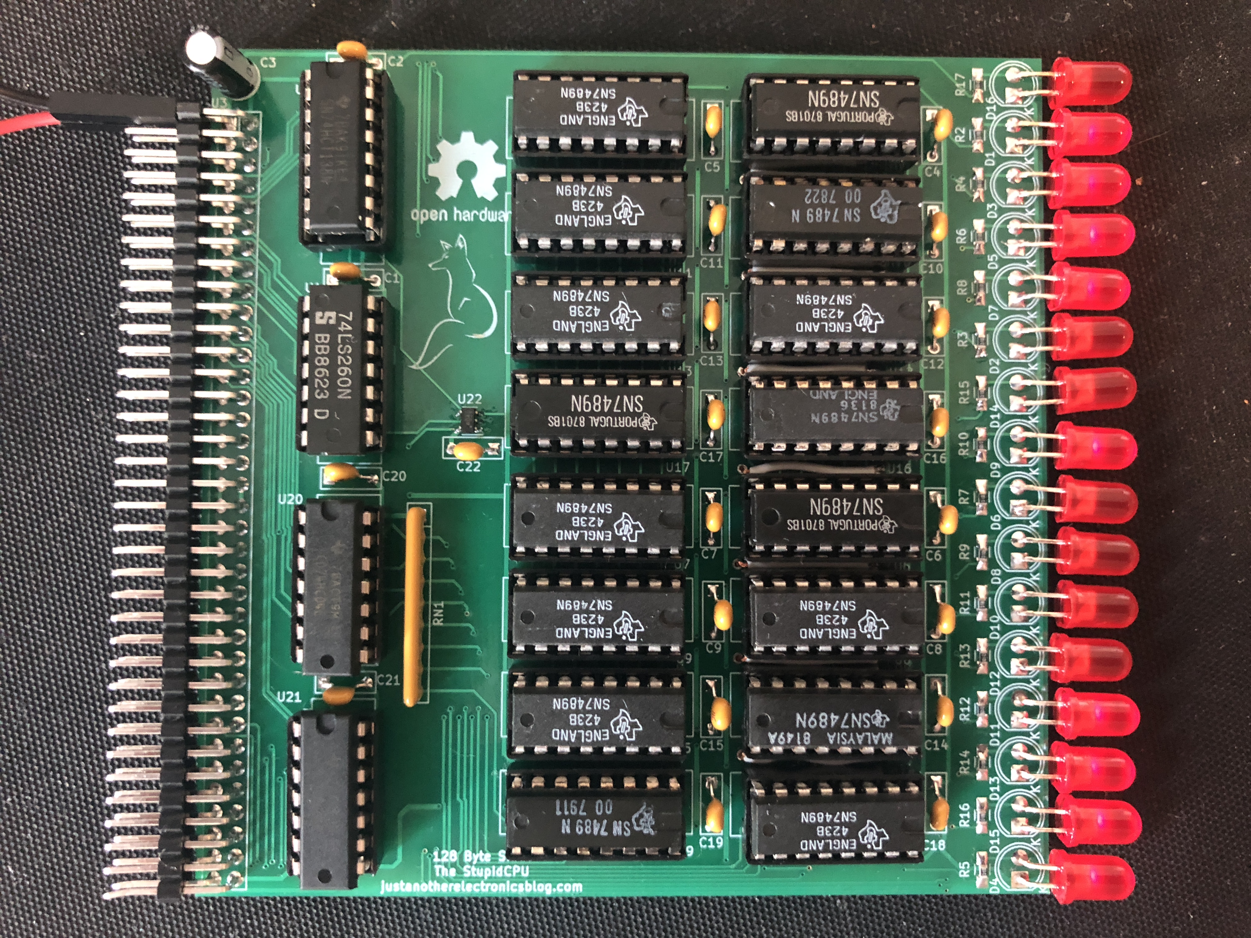
The array of LEDs clearly visible, as well as the 16 7489 ICs. When in use, the board needs over 1.1A at 5V to operate and gets hot to the touch.
A bug in the design was quickly found, the top 8 bits and not the low 8 bits of the Opcode where used, which was patched on the PCB.
Downloads:
The Kicad files can be downloaded here: RAMboard
Keep in mind, there is currently still a bug in the board, the final version will, when made and tested, be uploaded here as well
How do you get the SN7489N KiCad Symbol?
Heya. It looks like I drew it myself. It’s a fairly simple symbol, you can have a look here on how to add custom symbols:
https://techexplorations.com/blog/kicad/blog-kicad-5-recipe-how-to-create-a-new-component-symbol/