

I like CPU architectures, especially weird, interesting and unusual ones. For example, the Intel iAPX 432 is still something I would love to play around with. Recently, I realized that a working CPU can be made with just a simple Move instruction. For this to work, everything needs to be memory mapped. The ALU, program counter, everything.
Of course, this idea is nothing new and this idea is called the Transport Triggered Architecture. I decided to have a look into this, how it works and make a simple TTA CPU.
How does a TTA CPU work
Before I can make a CPU, let’s look into what is so different in a TTA CPU. In most CPU’s, calculations are done using registers and some arithmetic logic unit. For example, to add 2 numbers, the assembly code could be:
LOAD VARIABLE1, REGISTER0
LOAD VARIABLE2, REGISTER1
ADD REGISTER0, REGISTER1, REGISTER2
STORE REGISTER2, VARIABLE3
In a TTA CPU, there is no ALU or registers in the CPU itself. Instead, they exist somewhere in memory. In order to add 2 numbers, they are moved from memory or registers, to the ALU. The ALU result is then moved back to memory/registers. Or in code:
MOVE VARIABLE1,  ALU_A
MOVE VARIABLE2,  ALU_B
MOVE ALU_ADD_RESULT, VARIABLE3
In the simplest form, the CPU in a TTA CPU only needs to move data from one memory address to another. All calculations are done as a result of data being moved around. If you think, how would you jump to a different section of code, it’s easy. If the program counter is also in memory, a jump is as simple as moving a new address to the program counter.
A few TTA computers have been made, and even commercially sold. But in general, it’s a niche architecture that never has gotten popular. So let’s build one :D
Building a simple TTA computer
I decided to build the computer in Digital, a simulator for digital logic that is based on Logisim but much improved. Just the name is a bit too common when googling :)
In order to make a simple TTA computer, a few things are needed.
- A CPU capable of moving data
- A program counter
- An ALU
- A branch block
I want the CPU to be a von Neumann type of CPU, meaning that there is one memory bus with code to execute and RAM. To have a useable amount of memory, a 16 bit address, in order to address 64KB of RAM, is probably nice. Let’s just make it a 16 bit CPU when we are busy.
As there is just a single instruction, MOVE data from A to B, every instruction is 32 bits. First 16 bits with the address A, then 16 bits with the address B.
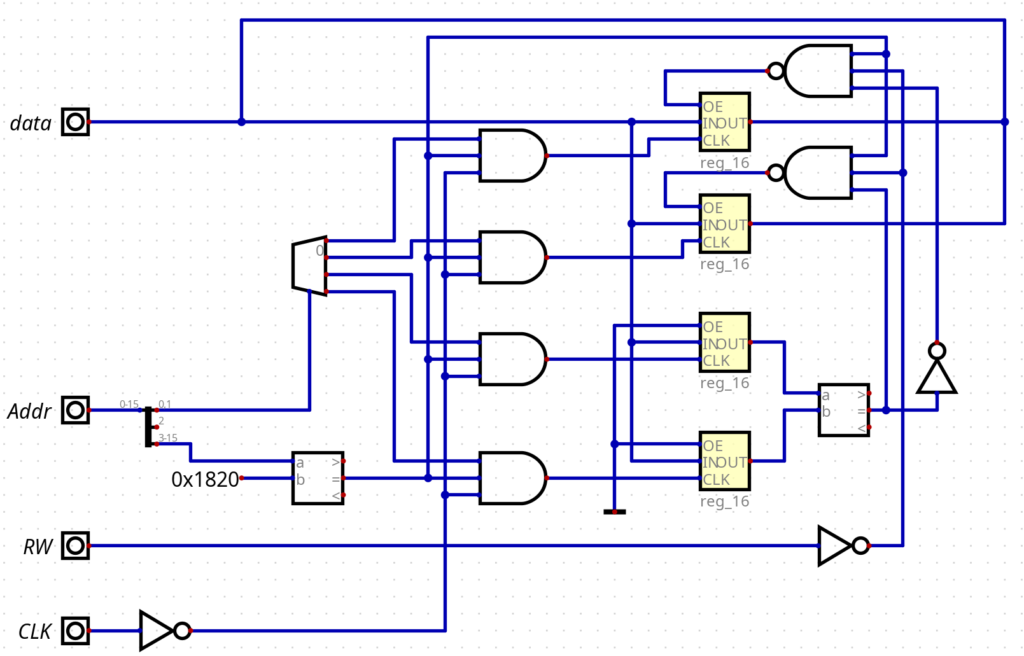
The CPU
The CPU can be surprisingly easy, after some consideration I came to the realization it just has to 4 things:
- Fetch the first 16 bits of the instruction for the source address
- Fetch the second 16 bits of the instruction for the destination address
- Read the data from the source address
- Write that data to the destination address
To build the entire CPU, a block to turn one clock signal into 4 is needed for the 4 steps. This means 1 instruction takes 4 clocks, but that is not too uncommon for a simple CPU.
The program counter is needed to select the right instruction, and a few latches or registers to store the addresses and data.
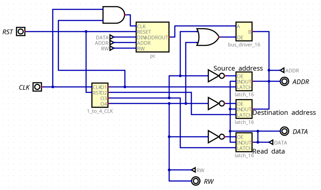
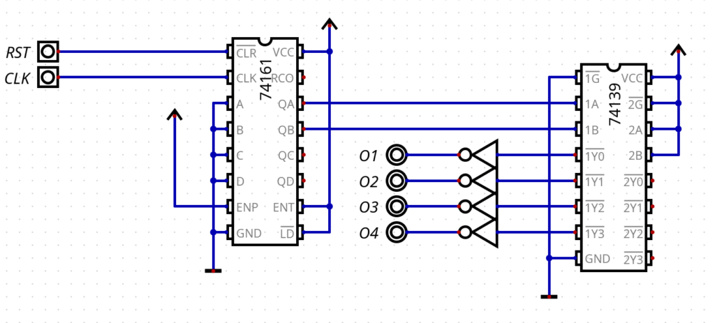
To simplify things, I created a 16 bit bus driver, 16 bit latch and 16 bit register building block. The 1 to 4 CLK modules is made using a 74_161 counter and a 74_139 2 to 4 decoder.
The program counter only sees a clock when fetching the instruction, when the CPU reads and writes to the fetched addresses, the program counter is not incremented.
The program counter
Without the program counter, the CPU won’t do much. To make a 16 bit program counter, a total of 4 of the 74_161 counters are needed. The program counter is, of course, memory mapped. In order to change it, a write to a specific address is used. This means a comparator is required to check if the address is correct. The output of the comparator AND the read/write signal are connected to the Load pins of the 74_161 in order to load a new value.
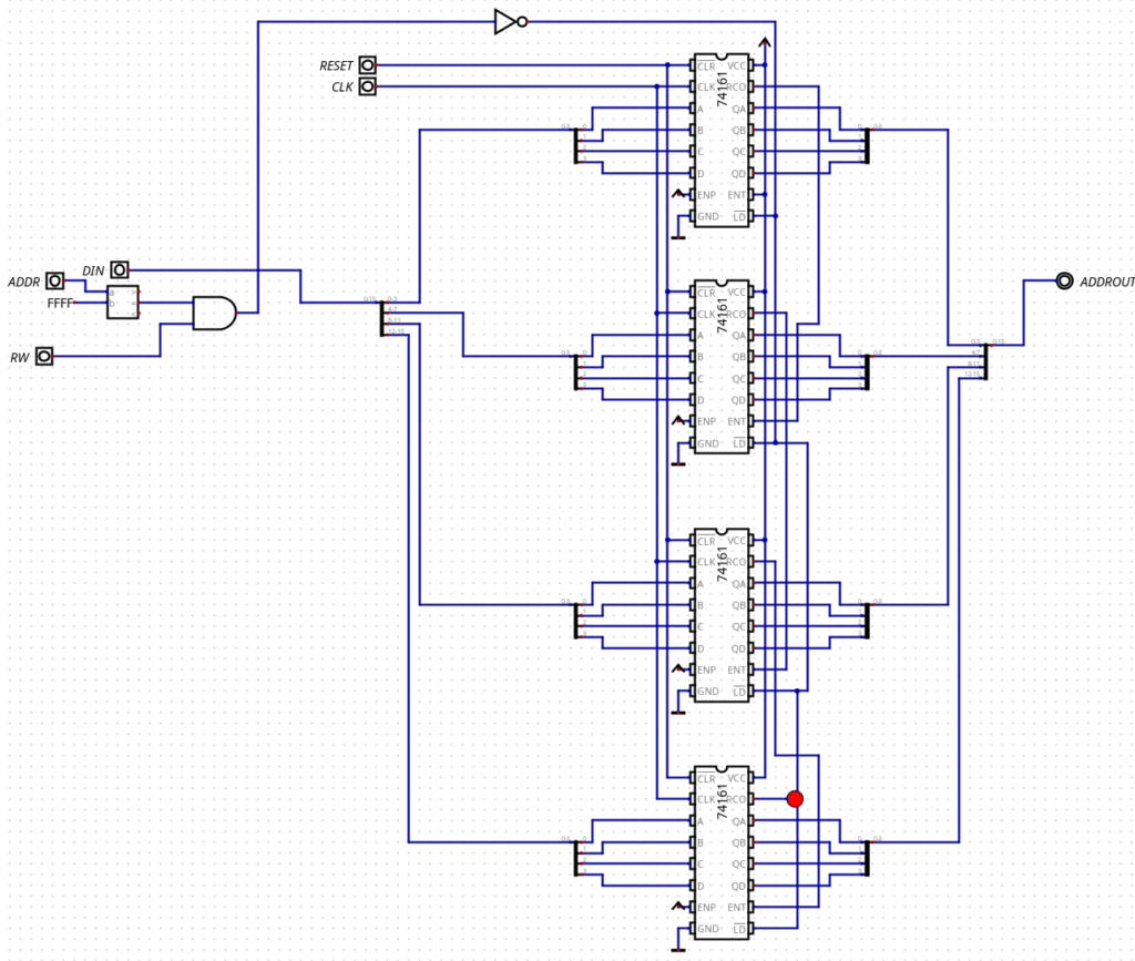
All in all, a fairly simple program counter.
The ALU
With the CPU done, let’s hook up some things to it, like the ALU
To keep part count down, a common option is to use the 74_181 4 bit ALU. With 4 of those, a 16 bit ALU can be made. Additionally, 2 registers are needed for the 2 inputs, and a bus driver in order to only output a value when needed.
Some logic is also required for address decoding. The lowest 5 bits select the instruction, as the 74_181 has 32 possible instructions. The 6th bit selects in which register to store the data for the input.
The full schematic is as follows
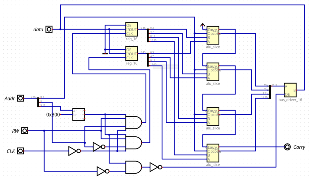
Each alu_slice just contains a 74_181, but connected in a way that I can work with busses. And even then it’s a bit of a messy schematic.
The flow control block
By lack of better name, the flow control block. Some form of program flow control is needed in order to implement something like an if() statement. In this case, a block with 4 registers and one output. 2 registers contain addresses, 2 contain variables. When read, if the variables are equal, address 1 will be returned, else address 2. And just like that, a simple flow control is implemented
A comparator, 2 to 4 decoder, some registers and addressing logic and that’s all. By now one downside of this type of CPU slowly pops up, having registers in all memory mapped peripherals like the ALU and flow control slowly make a small CPU fairly big.
With that all in order, the complete CPU looks like this:
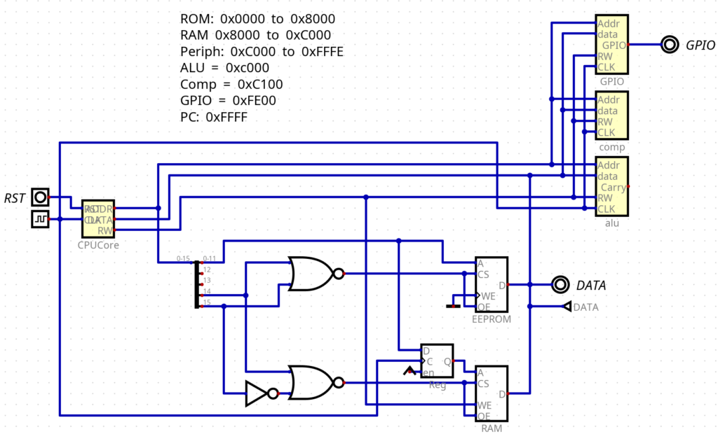
I added a GPIO block that just stores the value written to it to make debugging easier.
Let’s calculate some Fibonacci numbers
What to do with a simple CPU that does show it functions as a CPU? Calculate some Fibonacci numbers seems like a good idea. It’s simple, but does show some flow control and calculation abilities.
Let’s start with the code needed in C, or at least, pseudo-C, to calculate the first 10 Fibonacci numbers
int T1 = 0;
int T2 = 1;
int nextTerm = 0;

for(int i = 0; i < 10; ++i)
{
  nextTerm = T1 + T2;
  T1 = T2;
  T2 = nextterm;
}
Now, let’s translate that to a bunch of MOV instuctions. A big bunch of them. First, a memory map.
0x0000 to 0x7FFF is the instruction memory
0x8000 to 0xBFFF is the RAM
0xC000 to 0xC03F is the ALU
0xC100 to 0xC103 is the flow control block
0xFE00 is the GPIO block
0xFFFF is the program counter
//one time setup
MOV 0x64 0xC102    MOV 10, compareB
MOV 0x65 0xC101    MOV addrdone, Compare_addr2
MOV 0x66 0xC100    MOV 6, Compare_addr1
MOV 0x67 0x8001    MOV 1, T2

//Fibonacci calculation
MOV 0x8000 0xc000  MOV T1, ALU1
MOV 0x8001 0xc020  MOV T2, ALU2
MOV 0x8001 0x8000  MOV T2, T1
MOV 0xC012 0x8001  MOV ALU_O, T2
MOV 0x8001 0xfe00  MOV T2, GPIO

//handling the for loop
MOV 0x8002 0xC000  MOV CNT, ALU1
MOV 0x0067 0xC020  MOV 1, ALU2
MOV 0xC012 0x8002  MOV ALU_O, CNT
MOV 0x8002 0xC103  MOV CNT, CompareA
MOV 0xC100 0xFFFF  MOV Compare_O, PC
MOV 0x0065 0xFFFF  MOV addrdone, PC //just a loop
Wow, that’s a lot of code. Let’s try and unwrap that a bit. As the CPU can only move data, numbers have to be stored in memory. This means that the “int T2 = 1” C instruction is done by moving the value 1 stored in flash (in address 0x67) to variable T2 in RAM (address 0x8002)
The Fibonacci calculation itself is fairly easy, move T1 and T2 to the ALU, replace T1’s value with T2, move the result from the ALU back to T2. T2 is moved to the GPIO for a nice indication.
The for loop is handled by increasing a variable by 1 and comparing it to a set value, 10 (stored in address 0x64) for 10 loops. If they are not equal, the PC is set to the start of the Fibonacci calculation, else it’s set to an address containing an infinite loop.
Conclusion
And with all of that, it calculates.
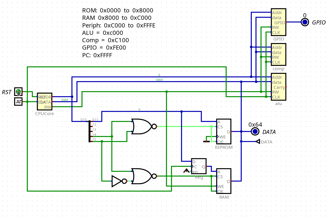
There is a small bug caused by the RAM being infinite fast and asynchronous, sometimes a value is written to address 0x8012, caused by the 0xC012 address of the ALU. Apart from that, the CPU happily runs along.
This was an interesting way of making a CPU, but it’s not the most efficient or fast CPU. It can be made pretty small however. All in all, a fun exercise in a quirky and niche CPU architecture.
All the source files can be found here, and if you enjoyed this post, you can buy me a coffee.
with chips
Hi,
a great post.
It would be even better, if you could replace the 181 with an ALU that can still be bought today
We have a MISC in FPGA, Steve Teal did it for me and it runs eForth
https://github.com/Steve-Teal/eforth-misc16
I would love to have it running in gates not simulator – speed is not an issue.
Kind regards
Juergen