

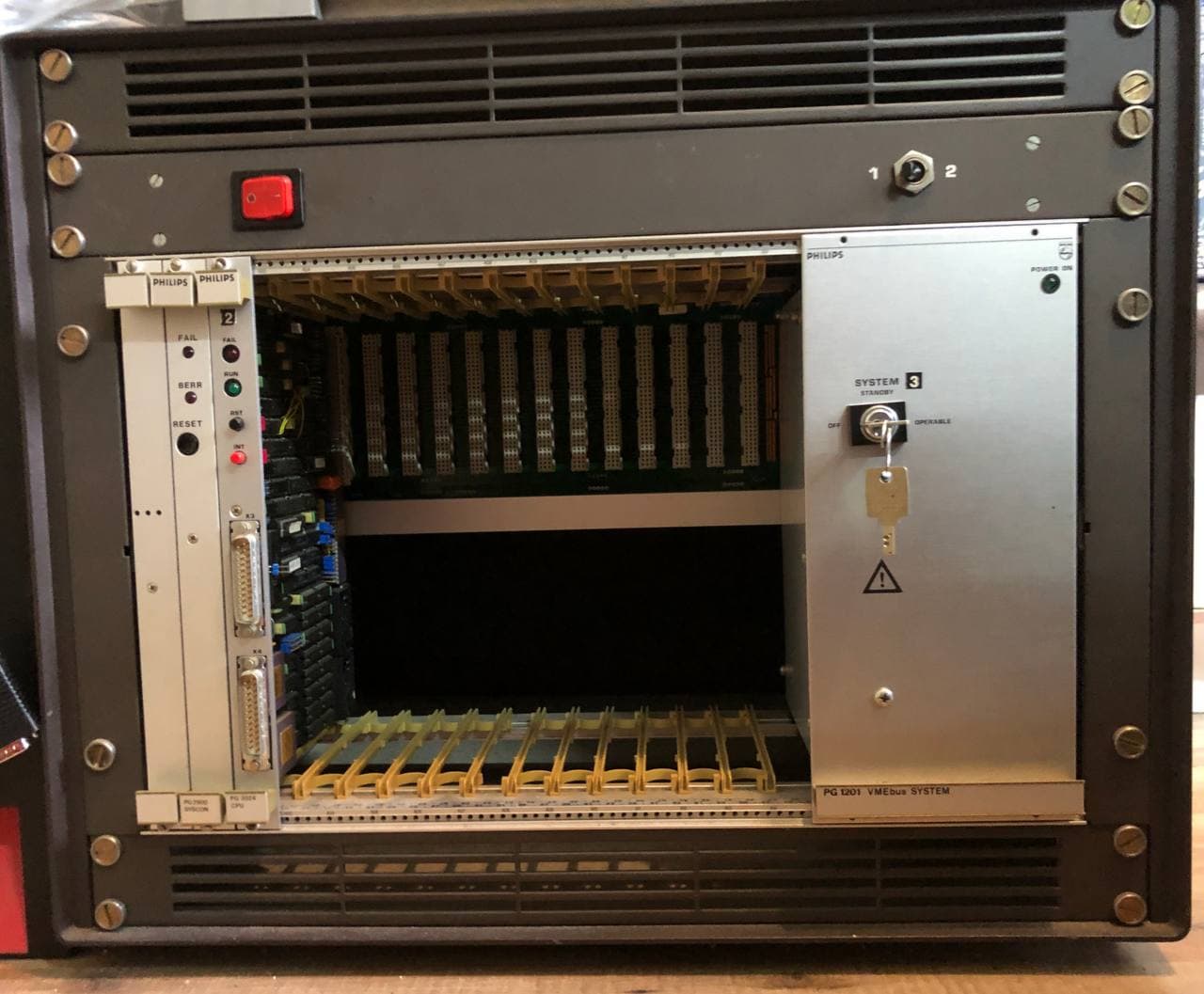
As I am still waiting on parts for the lab power supply, thanks 2021, time to look at something completely different. I picked up this giant box a few months ago. It contains a good old Motorola 68000 CPU board and a so called Syscon board all in a VMEbus backplane with plenty of empty slots. I could not find much documentation, apart from some Ebay seller selling the CPU board for a lot of money, as it was apparently used in an ASML system. So let’s dive into VMEbus, 68K assembly and some good old reverse engineering.
First things first, what is all on that CPU board.
A look at the hardware
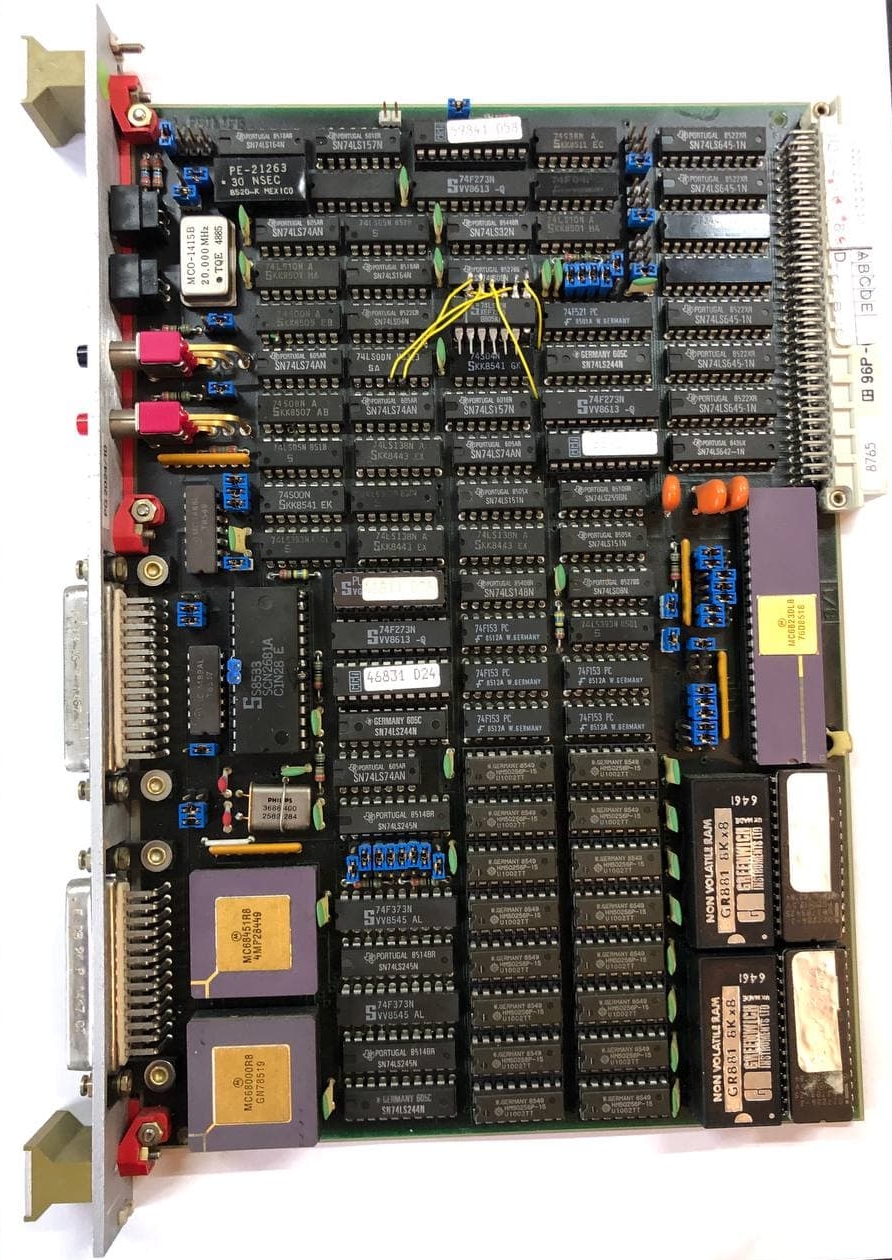
After some datasheet googling it seems that the CPU board contains the following:
- 68000 CPU
- 68451 MMU
- 512KB of DRAM
- dual UART
- Timer
- 2*32KB EPROM
- 2*8KB NVRAM
- Plenty of decoding logic.
Plenty of stuff on the board, most seem to be from the mid to late 80s. A lot of the chips have datecodes from 1985. A 32 bit CPU and 512K of RAM was comparable with a higher end PC back in that time so this probably was an expensive board. I am always unhappy seeing NVRAM. NVRAM is RAM with a battery inside to make it non volatile, but by now those batteries are most likely empty and the data lost forever.
The Syscon board contains a good handful of 7400 logic, nothing too special on here it seems.

VMEbus
So what is all this VMEbus stuff then? Simply said, it is a computer bus a little like our modern PCIe and a lot like the older ISA bus. VMEbus is a computer bus originally for the Motorola 68K that has seen use in industrial applications and in several computers and workstations. It contains most of the CPU signals of the 68K with additional features like multi master and interrupt lines. It is also an asynchronous bus, so no clock signal is needed. There must be one card that handles communications, who is allowed to be the bus master and such. This is what the Syscon card in the system is doing.
The monitor tool
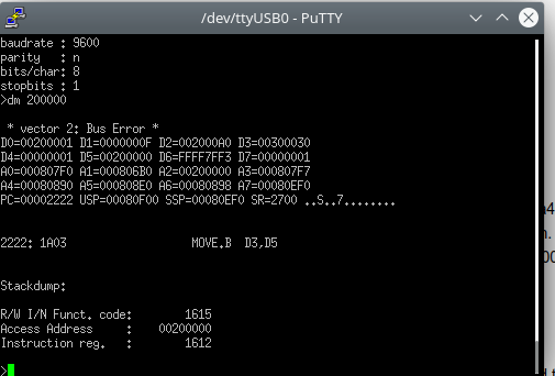
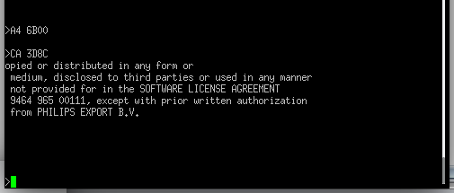
Now quickly back to that pretty pretty CPU board. I noticed that it has a UART chip and 2 connectors. Some tracing of the PCB later, it seems there are some level shifters between the connectors and UART and that the pinout is non standard. I decided to solder some pinheaders to the UART chip and just hookup a logic analyzer. I quickly spotted some communication on one of them, at the good old standard 9600 BAUD. After that I quickly hooked up a USB to UART converter and saw this:
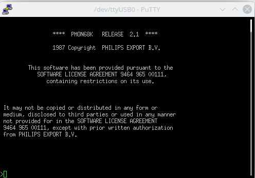
A monitor tool, that is a very good start. Monitor tools where commonly used to read and write to memory and sometimes to load, run and even debug code. Trying to enter a few commands like help, ? and run just gave me an error. After some good old keyboard mashing it seems that all commands are just 2 letters long. So instead of “help” the command is “he” And the good start is only getting better. The monitor tool supports a multitude of useful commands.
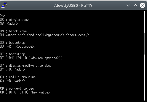
Some of the commands that seem the most useful are things like Single Step, Start Execution, Download, Display and Fill Memory, Display Registers, You can even set breakpoints. All in all this seems like an amazingly useful monitor tool. A few commands look a bit odd, like show process of soma, show mailbox of soma. They al do not run and throw an error that a ERM/DRM system is missing? Perhaps the NVRAM contained something nice that is now long gone.
I did read out the NVRAM to confirm and it is indeed empty. Curse you evil NVRAM!
A little look in the memory mapping
If I want to write my own code for this box, I need to know the memory mapping. Where the RAM, ROM and peripherals are located. So let’s try and figure all that out.
I poked around with the monitor tool, the Show Port commands shows there are 3 UART ports, which seems strange as I just saw a dual UART chip. So I poked around with the Display Memory command and the first 1MB of memory I can access. The rest, well:
The registers show that the stack pointer is located at 0x08F000 so the RAM is most likely located there. So the first MB of memory most likely contains the 512K RAM, the EPROM, NVRAM and perhaps peripherals. Time to dig a little deeper.
I dumped the EPROMs and had a look at them. As the 68000 has a 16 bit data bus, there are 2 EPROMs that together hold the monitor tool. After a quick merge together I had something that made sense. The file can be downloaded here for the people interested.
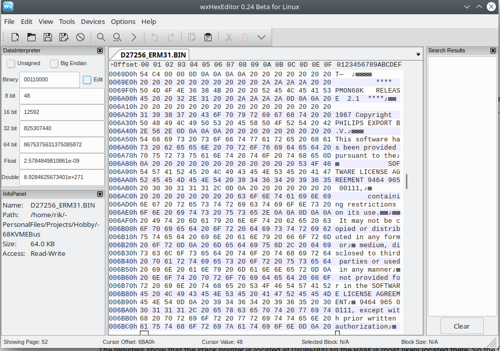
A little poking around with Display Memory and I found out the EPROM is mapped to address 0x000000 to 0x010000. One peripheral down, plenty to go. Time to fire up some more fancy reverse engineering tools.
A deep dive into the memory mapping
A while ago the NSA released Ghidra, a reverse engineering tool that also supports the 68K architecture. With Ghidra it is possible to look at a binary file, turn it into assembly, follow functions and much much more. Ghidra even tries to turn assembly functions in C. My plan is to look for the text printed at boot and hopefully trace that back to how UART and maybe some other peripherals are controlled. The message printed at start is located at address 0x69D4 and used in one function.
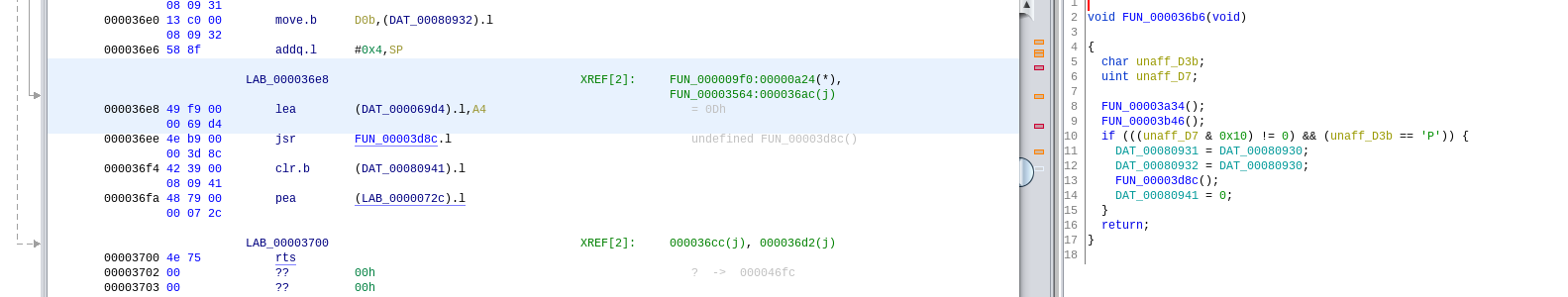
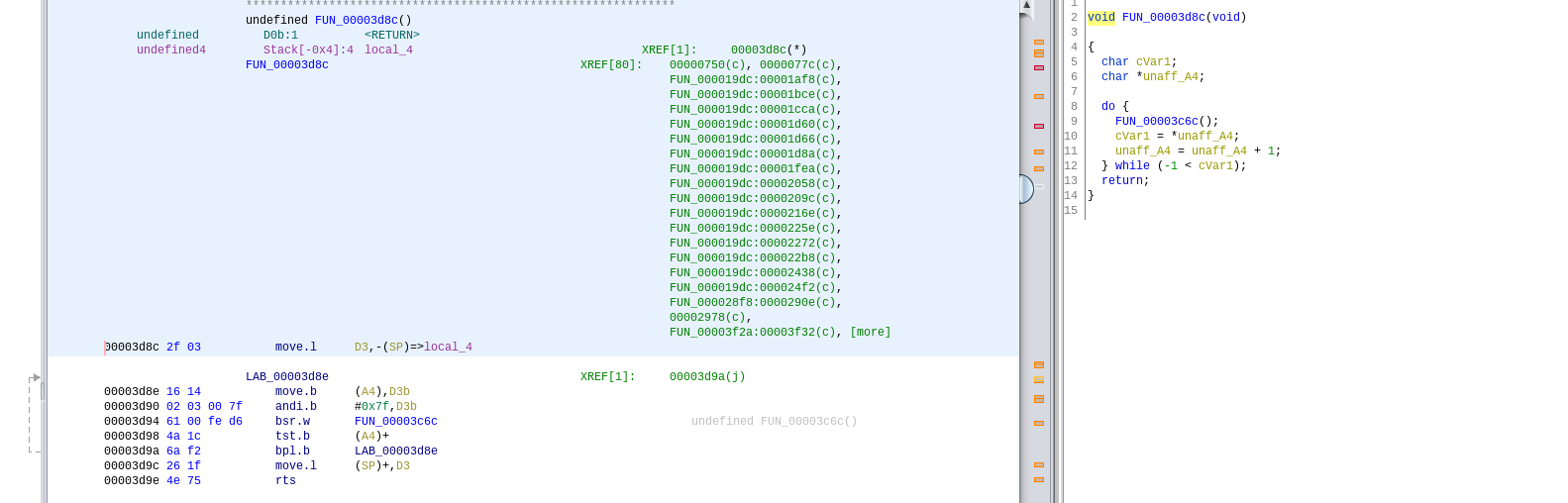
This function stores the address where the boot message begins in register A4 and then jumps to a function located at 0x3D8C. Now this function contains a do while loop adding 1 to register A4. That could very well be a loop that prints a character at a time. Or it could be something completely different as I never used 68K assembly before.
Luckily, I know a fun way to test it. If I load an address of a string in register A4 and just jump to this function it should print that. So I loaded an address somewhere midway of the boot string into register A4 and jumped to that function.
What do you know, it printed half the boot message. It indeed looks like that is a print string function. After looking at Ghidra for another hour and not learning much, I then decided to use the single step function and just stepped and stepped until I saw a single letter.
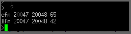
Apart from getting RSI from hitting enter a ton I noticed that ascii data was being moved to address 0x20040. 0x20040 is in register A1 and data, in this case the letter S stored in register D3, is moved to A1 + 7, a.k.a. 0x20047.
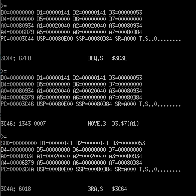
So to test this, I used the Fill Memory command to write a byte to this address, in this case the letter B. And what do you know, it works.
Looking at the datasheet of the UART chip, the peripheral is most likely mapped at 0x020040 to 0x020060. Another one down.
Though shall look at the second page on Google
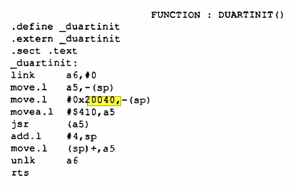
I spend another good amount of time looking and poking and staring a Ghidra. Eventually I got frustrated enough to finally resort back to Google and on the second or third page I found something. A thesis from someone using this exact same VMEbus box to control a robot arm. Luckily for me and sadly for people reading this, it was in Dutch. This document could have saved me a ton of reverse engineering time as it contains assembly code to control the UART and Timer. So remember, always look at the second page of the Google results. This confirmed that the UART is indeed on address 0x20040 and told me the timer is on address 0x200C0. It also mentions the 512K RAM is mapped from 0x080000 to 0x0FFFFF.
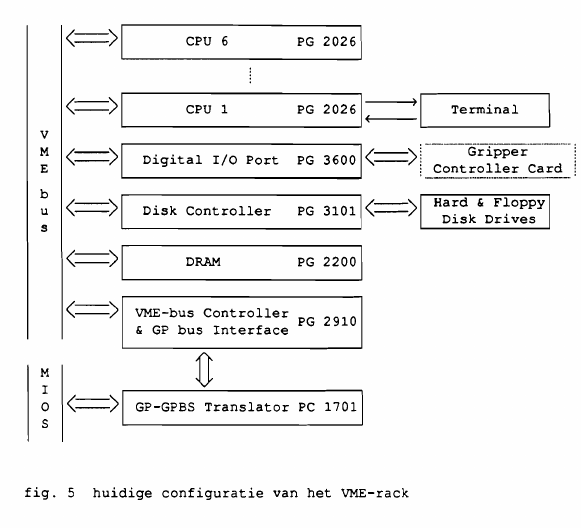
The system they used was pretty amazing for the time. They used 6 CPU boards, an additional RAM board, a disk controller board and a IO board. A machine with 6 32 bit CPUs, a total of well over 3MB RAM and the likes must have been a very pricey setup in 1988
The thesis also contains info about the CPU and Syscon board, including the meaning for some of the jumpers. One thing I could not find is where the MMU is mapped, or if it is even used. But with most of the peripherals now known, this was a very useful paper to read. The entire thesis can be found here.
The MMU
Modern CPUs have a MMU, Memory Management Unit, in the CPU itself. But back in the 80s it was common for this to be a separate IC. The memory address lines from the CPU go to the MMU and then MMU then accesses the memory. The MMU handles memory protection and can translate memory addresses. The latter is a potential issue when reverse engineering. For example, the CPU might access RAM at address 0x090000 but the MMU translates this to a completely different address.
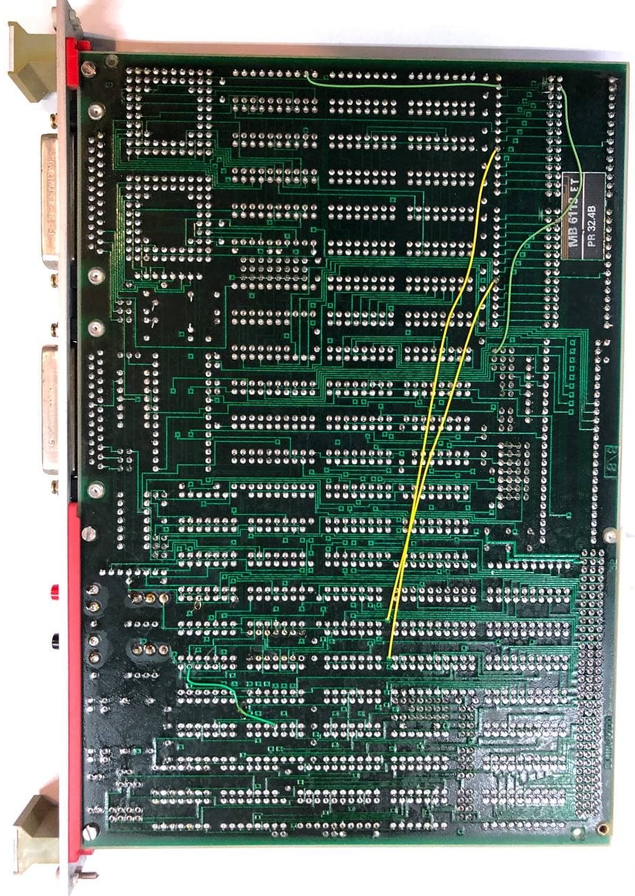
I wanted to figure out where the MMU registers are located in memory and check if it is used. Sadly I could not find this information in the thesis and poking around in Ghidra provided no clues either. So time to do it the old fashioned way and trace the address lines going to the MMU. As the PCB is a 4 layer job with a lot of traces covered by chips, I can’t see where everything is going by eye. So with my multimeter on conductivity setting, time to get going.
Tracing time
Generally, some of the address lines go into address decoding logic that outputs a single signal to an enable pin. For example, if a system has RAM on address 0xC000, address pin 15 and 14 could go to an AND gate and the output of that to the RAMs enable chip. So I started tracing the CE (Chip Enable) of the MMU and found that it went to a nearby 74S08, a chip with 4 AND gates. So time to trace the inputs of the AND gate. Input 1 went to the 68K reset pin and pin 2 to a 74LS138, a 3 to 8 decoder, another common address decoder chip. The inputs of this chip went to a 74LS244 buffer chip. Luckily, after all that the inputs of the 74LS244 went to some address pins of the 68K.
To be exact, address pin 8, 6 and 7. A bit more poking around revealed that the UART and Timer are also connected to this 74LS138. Some truth tables later and it seems that this 74LS138 is responsible for enabling the UART when address 0x40 is set on the bus, enabling the Timer when address 0xC0 is set on the bus and enabling the MMU when address 0x00 is set on the bus. As the UART and Timer are on address 0x20040 and 0x200C0 it makes sense that the MMU is then on address 0x20000. Most likely some more decoding logic enables the 74LS138 on this address.
Some looking at the memory on address 0x20000 and staring at the datasheet of the MMU later, I think the MMU is indeed located on address 0x2000 to 0x20030 and it seems to not be translating any addresses. Neat.
So will all that reverse engineered, the memory map so far is:
- EPROM 0x000000 to 0x010000
- MMU: 0x020000 to 0x020030
- UART: 0x020040 to 0x020060
- Timer: 0x0200C0 to 0x0200F0
- RAM 0x080000 to 0x100000
Running custom code
Finally time to actually execute some of my own code on this giant box. I spotted a few interesting commands earlier, called upload and download. Those seem usable to get some code into it that should be executable with the CA (Call Subroutine) command.
So the plan is:
- Write a very simple piece of code that changes a value in RAM
- Load this into the CPU board’s RAM
- Execute.
- Check if the RAM value indeed changed.
To write code, I used Easy68K, which is an amazingly nice program that can also emulate a 68K. This helped me immensely at the start. I also read the great tutorial on 68K assembly from MarkeyJester. Now it’s time to make my own code Luckily the assembly code for the first test is very simple:
ORG    $81000       ; start address
START:                  ; first instruction of program

* Put program code here
MOVE.L #$82000,a0         ; ram address to store data
MOVE.L #$12345678,(a0)    ; put some test data in RAM
RTS

* Put variables and constants here
END    START        ; last line of source
So, how to get code on the CPU board? I read somewhere in the thesis that the upload/download command support Motorola S-record files but I did not see anything happen when running them. Hmm, perhaps the second UART is used for this? Hooking up a second USB to UART converter and I was greeted with this:
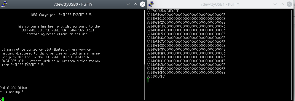
Very cool it can just output it’s memory content as S-Record. Let’s try uploading my own code. Easy68K also generates S-Record, so will it just work?
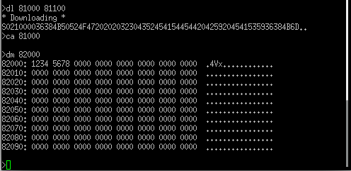
Executing the Download command on UART 1 and sending the S-Record file on UART 2 indeed just worked. So time for a quick Call Subroutine command and a Display Memory command to validate that it ran and what do you know, we can execute code
Blinking an LED
With the reverse engineering mostly done, I want to make an LED blink. This big box still has plenty of VMEbus slots unused, so time to add a card with some LEDs. A look at the VMEbus protocol later and this should be very doable. I would need some address decoding and a few flip flops to store data. If the address of my card is written to, store the data in some flip flops and use this to control a few LEDs. Easy enough right.

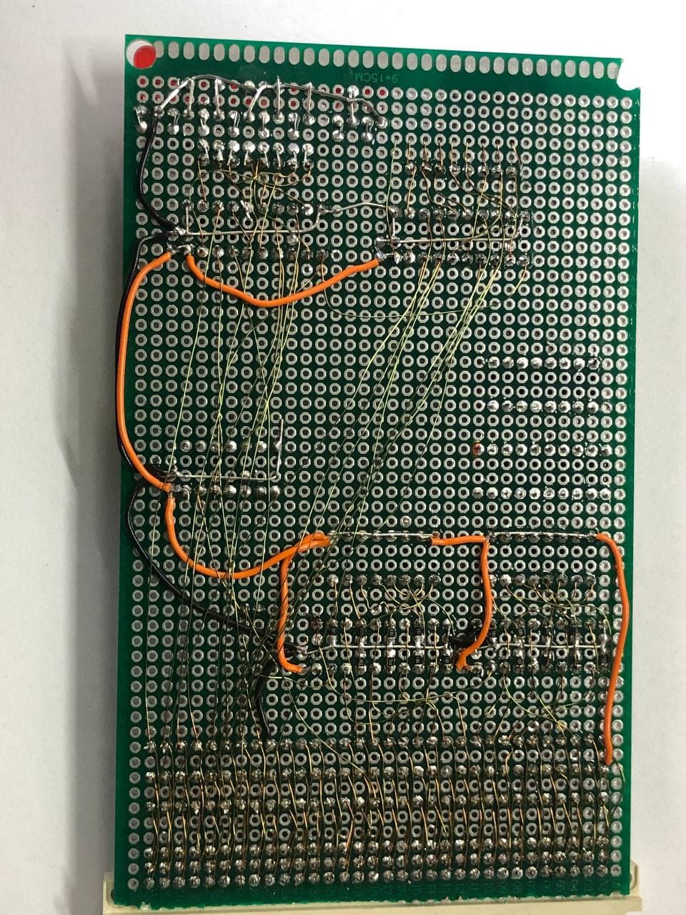
First I wanted to build a card with all the signals broken to pinheaders. Writing to any memory above 0x100000 gave a bus error. I hope the VMEbus is mapped to that area but I am not sure yet. So a lot of soldering later, I had this fun spaghetti like board.

And indeed, writes and reads to any address above 0x100000 are visible on the VMEbus. Great. Time to add some address decoding and some flip flops. I ordered some 74HC688 8 bit comparators and a few DIP switches. I still had some 74F374 8 bit flip flops. After thinking it out a bit I also found that I needed a inverter and a 74HC14 I had laying around will do. A rough schematic is here but it was all soldered without really designing a full schematic first.
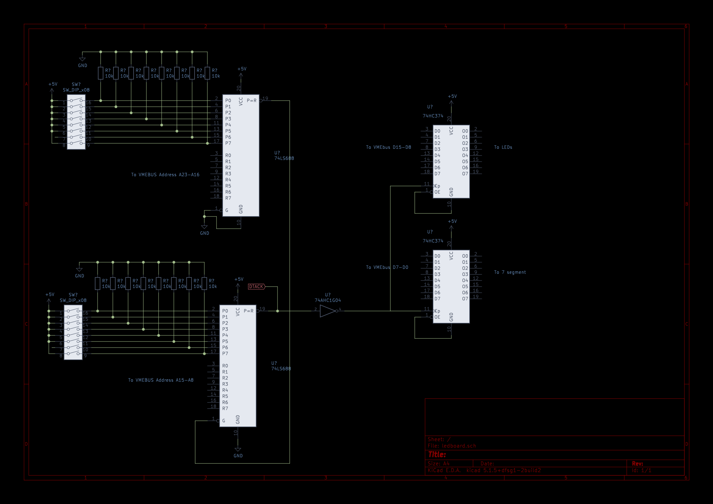
The 74HC688 comparators are daisy chained and provide a low pulse when the inputs from the VMEbus address match the DIP switches. This directly goes to the DTACK pin as acknowledge on VMEbus. It also gets inverted and send to the CP pin of the flip flops, causing them to clock in the data on the DATA pins of the VMEbus. I connected some LEDs and a 7 segment display to the outputs of the flip-flops.

So, the all important question. Does it blink?
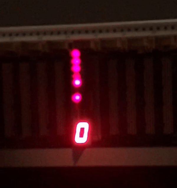
And it blinks very nicely. The assembly code for this is the following:
ORG    $81000
START:                  ; first instruction of program

* Put program code here
MOVE.L #$C00F00,A1  ; location of the LED card set with the dip switches

MOVE.L #$00000000, D4
MOVE.W #$00FF, (A1) ; clear displays at start, 7 segment is inverted as it's common anode.

FOR.B D0 = #0 TO #3 BY #1 DO.S      ; let's do 3 loops
    LEA SEGMENTLUT, A2              ; load the segment values address in A2
    FOR.L D1 = #0 TO #9 BY #1 DO.S  ; do 9 times for showing 0 to 9
    MOVE.B (A2)+,D5                 ; fetch the next segment value into D5
        FOR.L D2 = #0 TO #255 BY #1 DO.S ; the 8 LEDs count from 0 to 255
            MOVE.B D2,D4            ; D4 will be the value to write, first add counter D2
            LSL #$08,D4             ; leds are on bit 15 to 8, lets shift a bit
            ADD.B D5,D4             ; and then add the 7 segment value
            MOVE.W D4,(A1)          ; and write to the LED board.

            FOR.W D3 = #1 TO #500 BY #1 DO.S    ; a small delay.
        ENDF
    ENDF
ENDF

MOVE.W #$00FF, (A1) ;clear displays when done

RTS

* Put variables and constants here
SEGMENTLUT  DC.B    $C0,$F9,$A4,$B0,$99,$92,$82,$F8,$80,$90  ; 0 to 9 for the 7 segment

END    START        ; last line of source
Conclusion
It was fun and educational taking a dive into reverse engineering and using this fairly unknown computer from the 80s. I learned a lot about the VMEbus, 68K assembly and a bit on how to use a tool like Ghidra. As I know that the 68K CPU is capable of booting Linux and that a minimum 68K Linux system just needs a 68K, 512K of RAM and ROM and a UART, I might make a VMEbus card with some RAM and ROM and try if this giant box can boot Linux.
I hope this makes for an interesting blog, even if the chance of someone else having the exact CPU board is very slim. If you enjoyed this look at some 80s tech, leave a comment and consider buying me a coffee. I needed plenty of those when looking at Ghidra for this project :)
It’s very surprising to see a 68000+MMU combo. I was expecting to see an MMU only with 68010 based systems.
With a 68010 in the socket, you could really boot some old version of the Linux kernel.
On a 68000 you could boot uClinux though.
But you probably know all that already.
Yeah, the board I saw on ebay had no MMU but a PCB, most likely to just connect the addresses. So I reckon the MMU was optional. from what I read online, the 68K was used with an MMU at times, just not the 68451. If I indeed want to attempt to boot Linux, I might swap out the 68K for a 68010 yeah, though I am not sure if this MMU is even supported in the kernel at the moment.
My experience with the 68k family varied from 68008 custom sbc’s to several commercial vme bus boards from the 68000 to 68060 and everything between. My cpu cards came from Motorola, a company who’s name I can’t remember down in Huntsville, AL, and a company in Germany. Several custom vme boards, mostly i/o, were fun to do. Most of the systems ran IEEE488 instruments like impedance analyzers, power supplies, servos, digital (1k points) i/o, analog i/o, and other goodies to make or test electronic components. Since all my code started with a monitor I wrote in assembly, your assembly looks sort of weird since the 68k assembler I used did not really have for loops.That’s not bad, just different. There was a great company, SDS, that sold a very good C cross compiler that I still use to play around with 68332 stuff. Somewhere, I have several vme boards, all of whom are soon to be in a recycling bin. Great blog. The 68k and vme were interesting architectures and great for real time work.
Thanks for your comment, always interesting to hear other’s experiences with such systems. Easy68K adds the for loops, while loops and more, it’s not something other assemblers do as far as I know, but it does make it a bit more easy for beginners I’d say :)
Hey, Are you still playing with the mc68332?
The vme bus had some quirks. The backplane had jumpers for chaining irq lines and sometimes other stuff. Accessing a missing card would normally hang the bus and the cpu. One technique was to pump out a message during initialization announcing that the first access to a card was about to happen. If the system froze, it was an unresponsive bus card and the last message told the techs where the problem was. In a high noise environment, spurious exceptions happened. The technique for those was to fill every vector and log spurious interrupts. 68060 boards tended to be more sensitive to noise than 020 and 030 boards and proper grounding mitigated that. When Mot brought out the 040, the fpu radically changed and broke many peoples code. A float initialized to 0x0 caused an exception where earlier fpu’s did not and handled the conversion cleanly. Simple solution: initialize all floats to a floating zero before use. There were other gotchas. Having the fpus’s and mmu’s in a separate address space and an overall 16MB flat memory model made writing the rtos and real time code much easier. Context switches were highly chip dependent. Fun stuff.
I have 2 of these, new from 1990, still in the box with manuals if you someone is interested.
Hi Steve, I am interested! How can I contact you?
Hello sir ,
I have two MVME2305-900 Motorola boards
One is working as master the second as slave
The master one boot from external hard disk and working good the slave boot from the backplane
And didn’t work. I do many things but without results.
Please I need help
Thanks in advance