

In the last post I promised to talk about the custom hardware to drive the 64*64 LED matrix. I wanted custom hardware because my test setup looked a bit like this:
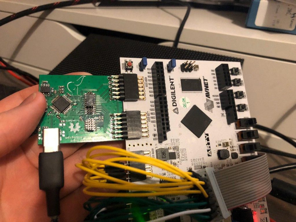
This is not ideal of course, and I want to use my dev board for other things as well. Hence the need for a custom PCB. In this blog I’ll be going over the design of the custom FPGA board to replace the test setup.
I came up with the following requirements for this PCB:
- FT232H for communication
I used an FT232H in the test setup above to get high enough transfer rates required for making gifs look nice. Each frame is around 12KB and to transfer 30 per second the transfer rate has to be around 400KB/second, something UART cannot easily do. The FT232H supports up to 60Mbit/sec using SPI, more than plenty.
- ICE40UP5K as the FPGA
The ICE40UP5K has plenty of on board SRAM, 1Mbit, is affordable and works great with the FOSS tools, perfect.
- 74HCT245 level shifters
I noticed some glitches in the test setup. It turns out these LED matrices need 5V IO. Hence some level shifting is needed.
The FT232H and ICE40UP5K need some additional parts, so the block diagram looks like this:
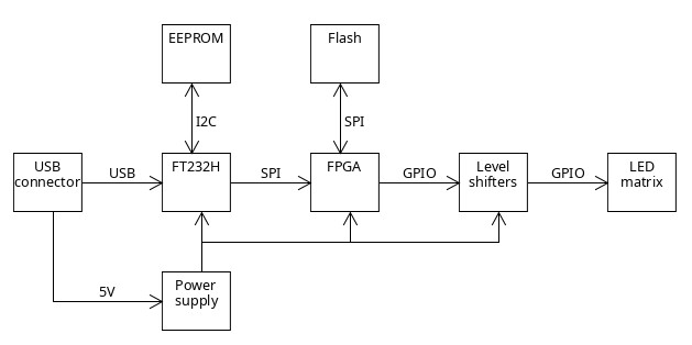
The FT232H needs EEPROM for it’s configuration and the FPGA needs external SPI flash to load it’s binary from.
Block diagram to PCB
Time to turn a block diagram into a circuit board. The full schematic looks like this:
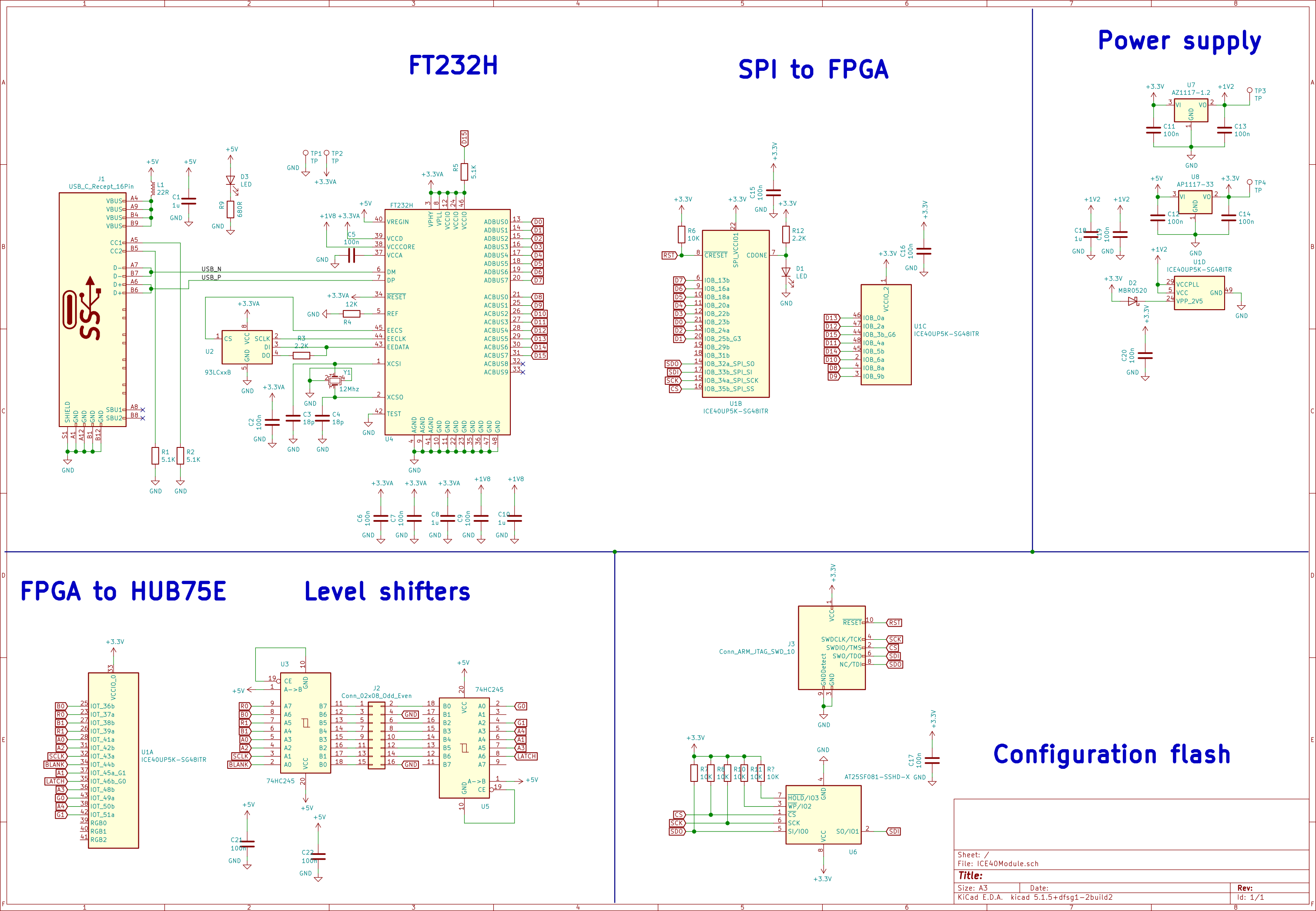
I like USB C, and luckily there is one USB C connector that is fully through hole. USB powers everything in this design, the FT232H generates it’s own 3.3 and 1.8V from USB. Several power supplies are needed for the FPGA, 1.2V for the FPGA core, 2.5V for the PLL and 3.3V for the IO. 2 linear regulars generate 3.3 and 1.2V and a diode lowers the 3.3V to 2.5V for the PLL.
I decided to just connect all the FT232 IO pins to the FPGA. Because the FPGA has enough IOs and because it might be useful in the future.
The LED matrix needs two level shifters for the 14 IO pins. Some SPI flash for the FPGA and a 10 pins JTAG connector later, the circuit is all complete.
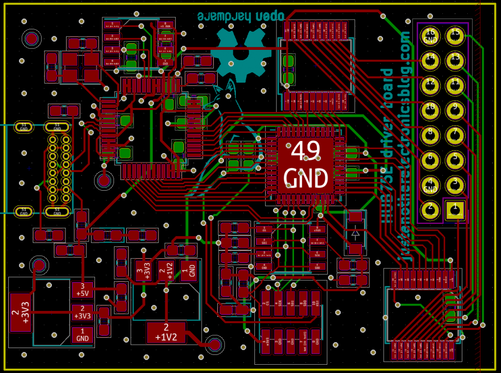
I turned the schematic into this PCB, a fairly compact 50x38mm board, all on 2 layers.
PCB’s
I already showed a picture in the previous blog post, now time for some more pictures.
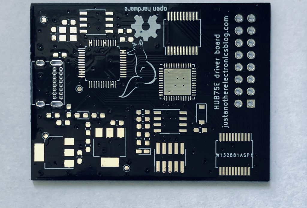
I ordered the PCBs from PCBWay in black to match the black plastic of the LED matrix. PCBWay offers a lot of options for PCBs, from fairly normal 2 layer boards like these to advanced 8+ layer or flex rigid PCBs. The PCB quality is good and the silkscreen is sharp enough for some smaller details like my logo. Moreover, the PCBs are affordable at 5usd for 5 or 10 pieces.
The downside of black PCBs is that the traces are a bit hard to make out. If you want to have very visible traces for easier debugging, green or yellow are better colour choices. However, if you want black, matte black has better visible traces but generally cost extra.
Building and bugfixing
So we have PCB’s, time to solder all components on it and give it a go. I generally solder the PCB block for block. In this case, I soldered the power supplies first and tested those. Secondly, I soldered the FT232H and surrounding components to verify that my PC saw the FT232. Lastly I soldered the FPGA and surrounding components.
This is where the issues began. I made several mistakes in the SPI Flash for the FPGA, basically having almost every pin incorrectly by looking at a wrong pinout. A lot of cursing and bug wire later, I have this horrid setup:
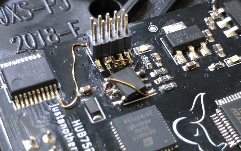
Not great, not terrible. Good enough for this project. I changed the schematic and PCB so the files online should be bug free. As I just want one LED panel on my wall, I have not re-ordered PCBs to test this :)
End result
After mounting the LED panel on the wall, I can now safely say this was a success.
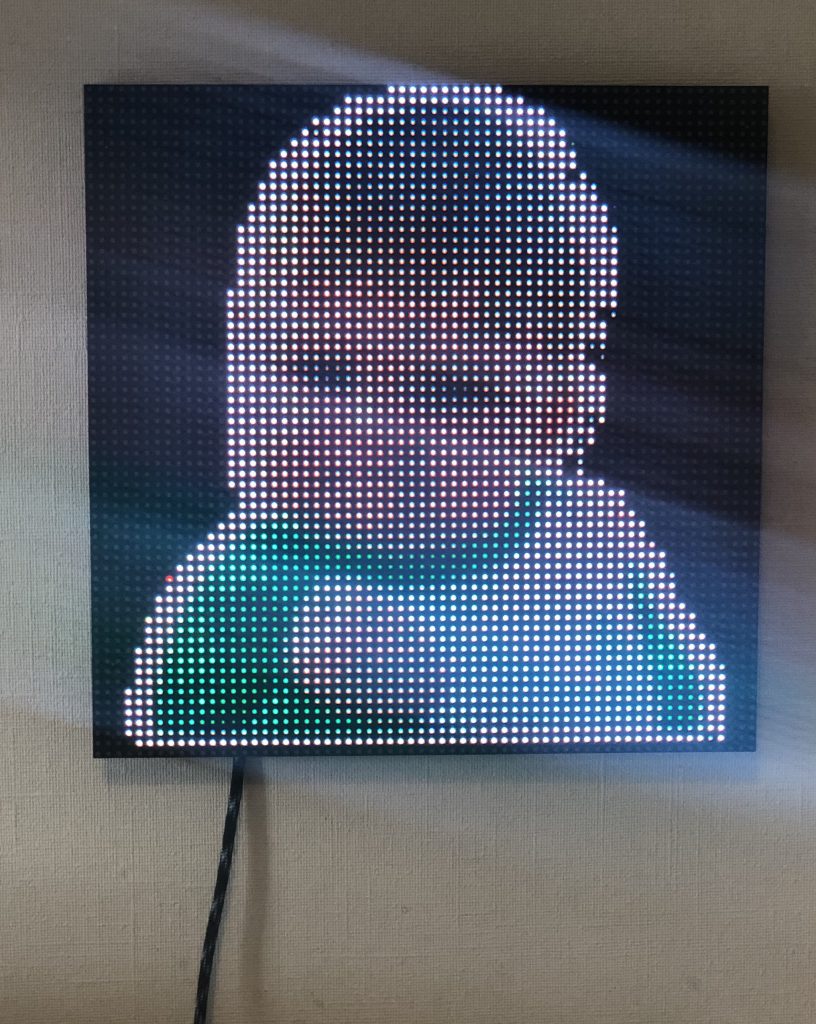
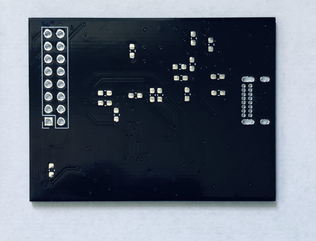
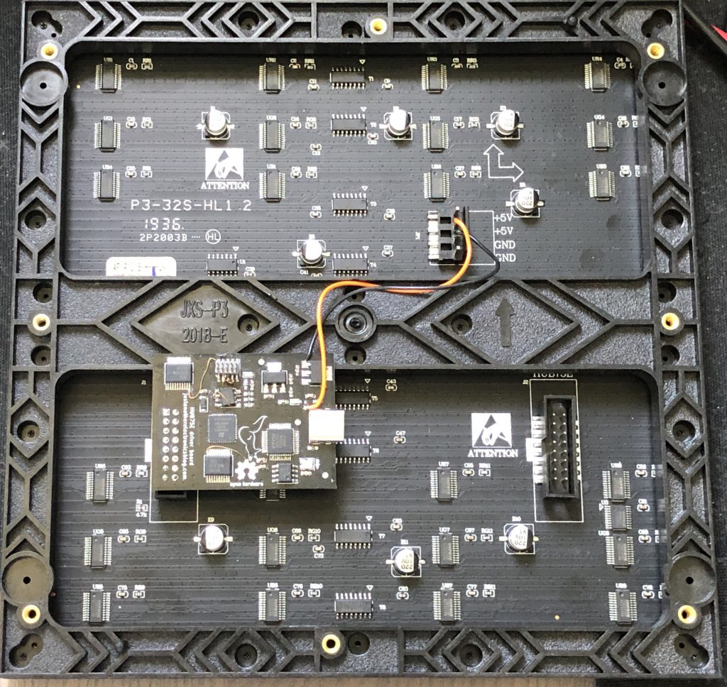
The backside looks like this with the module in place.
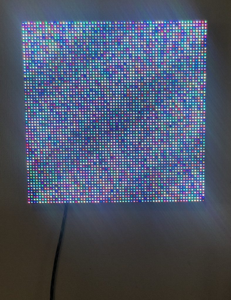
Something that I find kind of cool is that on a boot, the display shows what the initial value of the FPGA’s internal RAM is. This is always the same, but most likely differs per FPGA.
As always, the files are on Github. If you like this project and blog, you can always buy me a coffee.
Hi! quite impressing and complete solution to solve the heavy burden off a controller. Will try it out – and see if we might contribute somewhat.
Really nice project. But I’d suggest to use different level shifters, like 74AHCT541 – they have 3.3V compatible inputs, and can be powered from the same +5V as the LED matrix, separate from the rest of the board, without power supply sequencing issues. USB may not have enough power for all these bright LEDs, so they will need a separate power supply, and if powered down, will not clamp the FPGA outputs and load the USB port.
Oh those buffers are nicer yeah, I haven’t heard from them before, thanks :)
How the heck did you made the hardcoded SPI work on the FPGA? Could you send me any example?
What do you mean with hardcoded SPI, the SPI from FT232H to the FPGA?