

Sipeed is a China based company that makes all kinds of interesting dev boards for CPU’s and FPGA’s. I have looked at one of their boards before and recently saw that they released something new that looked like fun. It’s called the Sipeed Tang 4K. The name refers to a smaller FPGA board, the Tang Nano. The Tang 4K however has an FPGA with ~4000 LUTs instead of the ~1100 of the Tang Nano. At around $20 it’s also very nicely priced and comes with some interesting features.
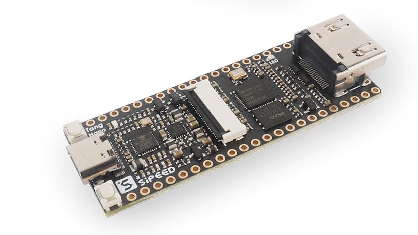
The most obvious one is the HDMI port. Sadly 4K video is not going to be possible with this, but their example does a very respectable 720P. Having HDMI is really nice in my opinion as driving displays is a great showcase of something an FPGA can do compared to a microcontroller.
Looking a little further, more and more fun stuff started popping up. The Gowin FPGA on this board has an ARM M3 core with some peripherals build in, as well as 8MByte of HyperRAM, 8MB of PSRAM and 4MB of NOR flash. Even without the FPGA, an ARM M3 with that amount of RAM and flash is pretty impressive.
So let’s look at using it and adjust a few existing FPGA projects to run on this FPGA.
The programming environment
The Gowin FPGA on the Tang 4K can be programmed using the proprietary Gowin IDE, though an open source toolchain is being worked on. The Gowin IDE is free, but it needs an account and a license to function. Luckily the latter is provided within a few hours in after requesting it. The IDE itself is a fairly small at around 1GB installed, at least compared to Vivado/Quartus program. It even worked on Ubuntu 20.04 without any issues:
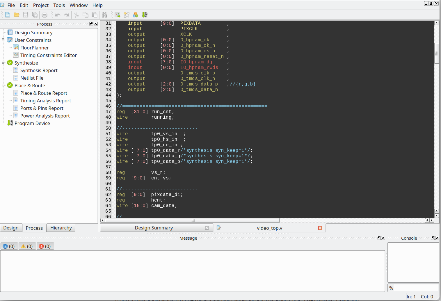
Compared to other vendor IDEs, this one is actually pretty simple to use. When loading an example project, 3 tabs can be found. Design, Process and Hierarchy. Design contains all the files and info on the selected FPGA. Hierarchy contains the HDL files in hierarchical view, when there is a design error, it will state so. After synthesizing it also contains the resource usage per file.
Finally Process, which contains the Synthesize, place and route and program device stuff. Double-click on each to start this task and a minute later it’s done, at least for a small example. All in all I find it a fairly simple and usable IDE. Of course, like all FPGA IDE’s, the build in text editor is pretty bad. But at least there is a dark theme :)
The example projects
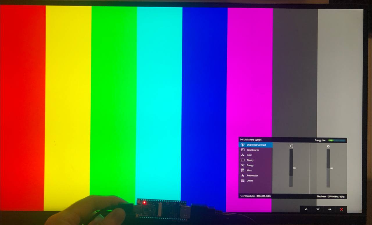
There is a github page with exactly 2 examples. The ubiquitous blink a led example, and an example that generates an image inside the HyperRAM and uses the HDMI to output it. That sounds a lot more interesting, so let’s run it!
That looks fun. Let’s have a little look at how it works!
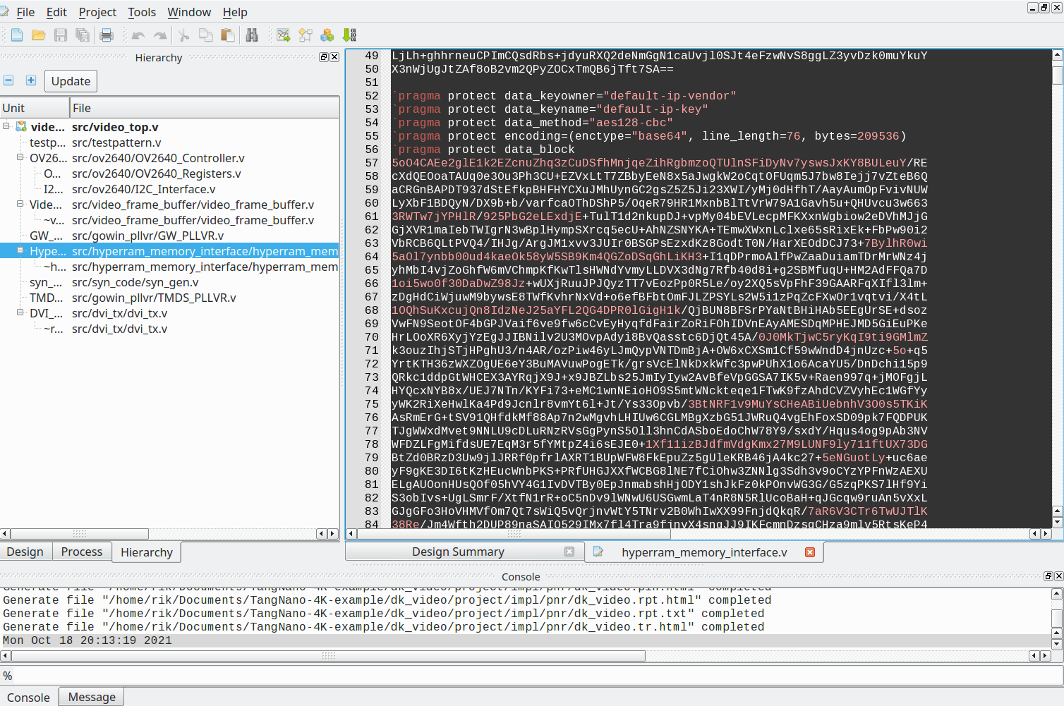
Oh, encrypted blobs of verilog for the HyperRAM, HDMI and framebuffer. That’s not fun :(
I think we can do a little better then that. Since I started tinkering with the FPGA, someone else made a cool project with this board, a gameboy to HDMI adapter, though it also uses some encrypted verilog for the HDMI part.
Using the HDMI
HDMI has been implemented on FPGAs quite a few times before, though a reasonably fast FPGA is needed for directly outputting HDMI. I found this project online, which supports several FPGAs. So let’s port that over to the Gowin FPGA. Now, just HDMI is a little boring, much nicer if there is something cool to show on the screen.
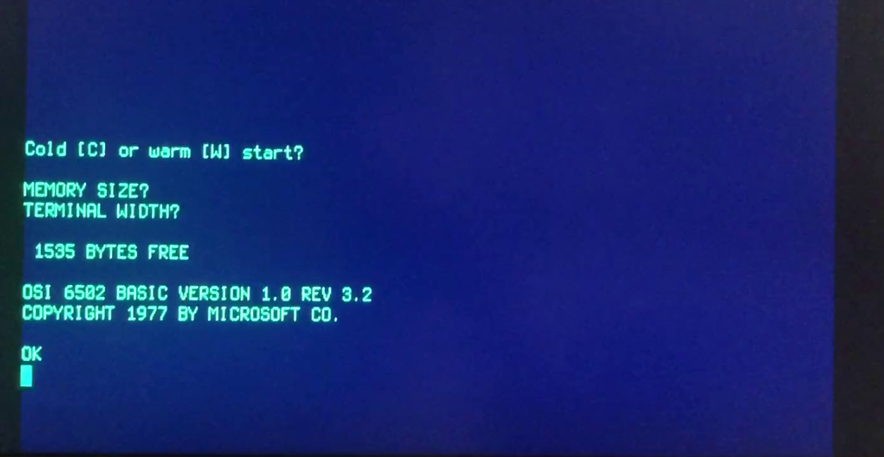
I always liked the idea of a simple BASIC computer, like the 6502. There is a nice FOSS project with the 6502 on an FPGA from Grant that could work. So the idea is, run a 6502 computer that boots BASIC with HDMI out on a small FPGA board. Even better, I just need to hookup a few already existing projects, easy enough right? Right?
I started with just getting the HDMI to work. Luckily there is a porting guide for the projf display controller. A PLL is needed for the HDMI clock, as well as serialization and differential signalling. The porting guide mentions 10:1 serialization for HDMI, and this is something the FPGA can luckily do. Gowin has a nice document describing all the IO modes and is full of sample Verilog and VHDL snippets, great!
The FPGA should be capable of 720P, so let’s go for that. The clock speed needed is 74.25Mhz, but as the data is clocked out serially with 10 bits per clock, the clock speed on the IO needs to be 742.5Mhz. That’s quite something. Luckily this is done via the 10:1 serializer, which needs 5 times the base clock. Just a comfy 371Mhz needed. I used the PLL and clock divider wizards from the IP wizard tool in the IDE, which happily generated this.
After adding the code for the OSER10 serializers and the TLVDS_OBUF DDR outputs, this all worked without too much issues.
I optimistically tried 1080P, which gave a lot of timing errors and well, there was an attempt let’s say :)

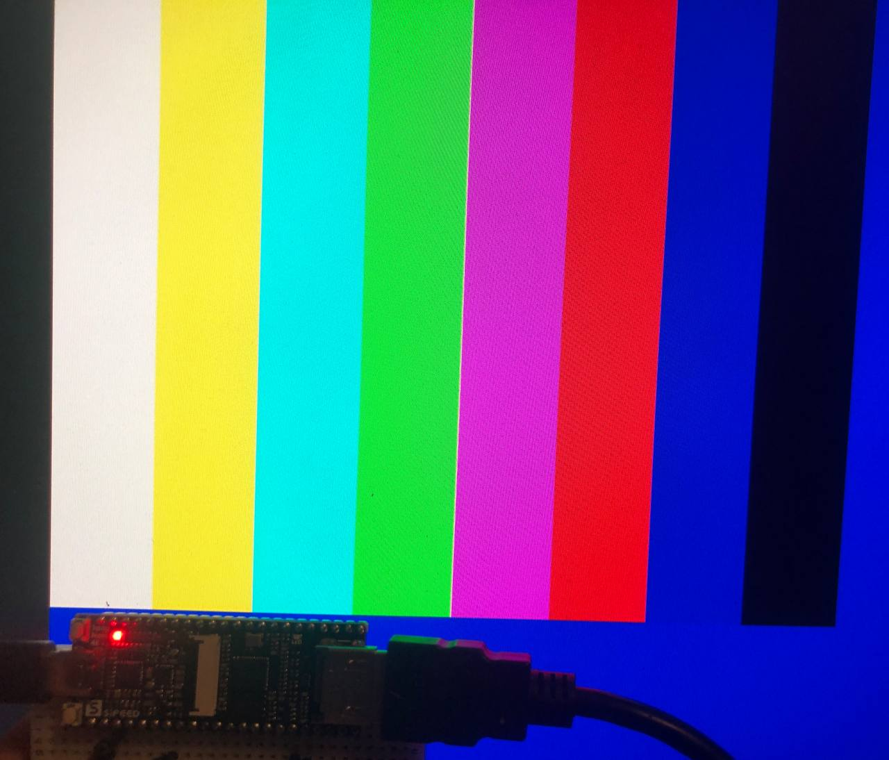
Perhaps 900P is possible, but I haven’t tried. But with HDMI up and running, let’s look at that 6502!
VGA and HDMI timing issues
The 6502 page describes a few example projects with VGA output, even color VGA. So all I have to do is hook it up HDMI and BASIC like it’s 1977 right> Sadly it is a little more complicated then that. To output VGA, almost all projects generate their own VGA timings, And for HDMI, the display controller generates it’s own timings. Converting that to HDMI is a little complicated
After fighting around a bit, I decided to approach it a little differently. I opted for the 6502 computer with serial out so I can test that with a USB to UART converter to my PC first, and then add a terminal emulator and botch HDMI to that. I messed around with this great VT52 FPGA project before and was familiar with it’s code. Eventually I ended up matching the VGA timings in the VT52 with the HDMI timings until it worked. Not a great solution, but workable for now.
A better approach would be to completely replace the VGA parts, but perhaps for another time. For now, I am really happy being able to BASIC:
I exported the project to Github, it should be possible to directly open it in the Gowin IDE. The resulting binary is also included. To use this, a PS/2 keyboard needs to be connected to the FPGA. The PS/2 clock to pin 14 and the PS/2 data to pin 33. A level shifter is needed but for me it worked fine without for a while.
A RISCV CPU with HyperRAM
That’s HDMI up and running, let’s have a little look at the build in HyperRAM. First, what is HyperRAM?
HyperRAM is pseudo-static RAM, meaning that internally it’s DRAM, but with a controller that handles all the annoying DRAM stuff. The databus is 8 bit wide, so the number of pins needed is quite small. It’s popular for hobby FPGA projects because of those reasons. Generally it’s available in 8 MByte chips, but bigger capacities exist.
Gowin decided to just add some into the FPGA, most likely by having multiple die’s in the IC package. I wanted to work with HyperRAM for a while now, so that seems like a great excuse. There is also some PSRAM inside the FPGA as well, but let’s focus on HyperRAM for now. They sure have filled this chip to the brim with goodies.
RISC-V time
So how to test that memory, having a CPU to read/write data and print out the results to UART seems like a good choice. But what CPU to pick? I have done a whole blog about it, but I’ll pick one I haven’t covered yet, the NEORV32. It’s based on the NEO430, but with a RISC-V core. I really liked the NEO430 and so far the NEORV32 is even nicer. It has wishbone support and the base SoC is very complete and easy to use. The bootloader they offer is also a real life saver, and NEORV32 also supports optional hardware debugging.
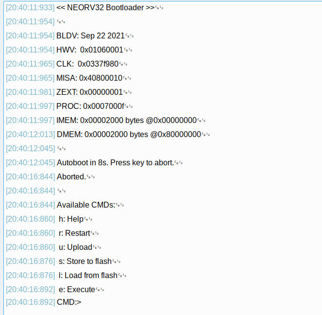
There is a small downside, it doesn’t fit. The FPGA has 10 memory blocks, but to implement a 32 bit RAM or ROM that is also accessible per 8 bit word, 4 of those blocks are needed. With RAM, ROM, the bootloader and registers in RAM blocks, 12 would be needed. I tried to implement the registers in logic cells instead of RAM blocks, while costing a lot of logic at least the CPU would fit like this. In the end I opted to use the RISC-V e extension, which cuts the general purpose registers down from 32 to 16. With this implemented I only need 10 RAM blocks and around 70% of the FPGA’s logic cells, perfect.
Adding the RAM
Gowin recommends to use their own library, but in their documentation they list that the HyperRAM used is a Winbond model, most likely this one. They also go into some detail on how to use the HyperRAM.
In order to connect to the RAM, the top level should have the ports for the RAM with the correct names. The synthesizer will then deal with it and magically connect it to the RAM, neat.
  port (
    O_hpram_ck      : out std_logic_vector(0 downto 0);
    O_hpram_ck_n    : out std_logic_vector(0 downto 0);
    O_hpram_cs_n    : out std_logic_vector(0 downto 0);
    O_hpram_reset_n : out std_logic_vector(0 downto 0);
    IO_hpram_dq     : inout std_logic_vector(7 downto 0);
    IO_hpram_rwds   : inout std_logic_vector(0 downto 0)
  );
Now to add a HyperRAM controller, A popular open source HyperRAM controller is this one from Blackmesa labs, which should work nicely. And even better, Greg Davill made a simple wishbone wrapper for it for the bosonFrameGrabber project. So let’s hook that all up to the CPU and give it a go. I ran into a few issues, like the reset for the CPU being active low and HyperRAM being active high. But it was all communicating rather quickly. Good to note is that the CPU is written in VHDL and the HyperRAM controller in Verilog, the tooling has no problems mixing these two.
I made some simple code to read and write to the HyperRAM, and also added the RAM to the linker file so the CPU can use it as RAM. With a 54Mhz CPU and RAM, the read and write speed is around 12.5Mbyte/sec. Considering the HyperRAM controller is made for simplicity and not speed, this seems very reasonable.
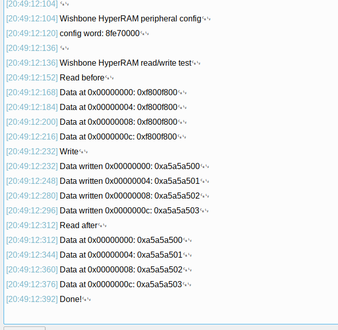
This project can also be found on Github and requires a serial to USB converter to be connected to pin 22 (RX) and pin 23 (TX)
Conclusion
There are a lot more interesting things in this FPGA, another 8MB of RAM, NOR flash and an entire CPU. But for now, having 2 projects working with a lot less encrypted verilog seems like a good start. A lot of work being done on the open source toolchain, I am curious to see where that leads to in the future.
I hope these projects can help others get going using this interesting FPGA board. If you enjoyed reading this, consider donating me a coffee!
Thanks for this great article.
I’m the author of GbHdmi project, then, it’s possible to use Chisel not encrypted HDMICore now :
https://github.com/Martoni/HdmiCore
Just add the option when generate verilog for GbHdmi project :
$ sbt “runMain gbhdmi.TopGbHdmiDriver noGowinDviTx”
@+
Thanks, I completely missed that, nice to hear you got it working without the blob as well :)
I am wondering if this can run a Monero full node and if the FPGA is large enough to hold a mining algo? I’m sure it would be slow as hell but it would be pretty cool to run one on a cheap fpga that I could play with the fpga to try to mine randomX
Heya, I don’t know much about how Monero works internally, but from the looks of it that would be very difficult at least. I know there are some open source bitcoin miner projects for FPGA’s but those also need a bigger FPGA to run.
Thanks for the reply, I most interested in just hosting a node on as small a footprint as possible.
Mining is a just a secondary thought as this looks like a cheap entry into learning fpga programming.
Hdmi patterns for nano 4k
https://github.com/splinedrive/my_hdmi_device
Examples with free hdmi under
https://github.com/splinedrive/TangNano-4K-example
Ah thanks, looks nice :)
Thanks for this blog post, it’s really interesting. I noticed that Sipeed are about to release a Tang 9K (see their Twitter feed). :)
Oh neat, thanks for the heads-up!
Hi. I am evaluating this board. Looks interesting, I could already do a couple of things, for example, I have implemented Z80 core and simple character screen in it.
I have a question. Did you try the hyperram controller provided by the IP core generator? I cannot make it work. init_calib signal never goes high. Can you help? Do I miss something?
Heya, thanks for the feedback. I haven’t tried their Hyperram controller so I’m afraid I cannot help you with that.
I had the same problem using psram (init_calib stays low). It seems to be a problem with the 2.0 psram IP. Just use version 1 instead. I’ve shared an example at https://github.com/zf3/some-tang-nano-9k-examples.
You can do 1080p, but not at 60Hz. I tested 24Hz and 30Hz and they work perfectly. VT52 goes crazy though.
You can do 1080p, but not at 60Hz. I tested 24Hz and 30Hz and they work perfectly. VT52 goes crazy though.
BTW, that BASIC just turned 50. :-)
Oh cool, thanks for the heads up. Something to try soon then, 1080P from an affordable FPGA is pretty amazing :D