ECL logic ramblings

ECL logic, or emitter coupled logic is a family of very high speed logic. with ECL logic, a transistor is never completely on or off, meaning the transistor is never saturated, making it very fast. It also makes it weird and quirky, interesting enough to have a look at. First of all, ECL logic generally works on -5V instead of 5V, though later it was also available using a more normal 5V power. Second of all, the logic level is not 0V and -5V, but roughly -0.8V and -1.6V. Third, most ECL logic has 2 outputs, a normal and an inverting one. This can be used to make logic design easier or to have an differential pair output for noise immunity. ECL was used in multiple well known designs, for example the Cray-1 supercomputer used ECL.

All in all, interesting devices. The easiest way to experiment with them is by buying some logic devices. ON semiconductors still makes them, the NC10EP01 for example is a single gate OR/NOR that can be used with 5V or -5V as power supply. It’s a very fast device, reaching over 3Ghz switching speeds. The datasheet can be viewed here.

But where is the fun in that, it’s much more fun to make a few gates. The schematic for a NOR gate is easy to find, it’s even listed on the Wikipedia page about ECL. I changed the schematic a bit to make a 4 input NOR. I also made an SR latch based on the design found here. The schematic for the NOR gate is:

Continue Reading


The StupidCPU, an 8 BIT 7400 computer, part 1, the architecture.

Another day, another silly DIY computer.
Making a computer from scratch is a popular project, whether it’s done with an FPGA, an older CPU like the 6502, discrete logic like the 7400 series or even with just a big bag of transistors, so time to give it a go as well.
A good couple of years ago I designed a very simple ALU as a school project, but never did anything with it, so time to change it.
As it’s a horribly inefficient 8 bit CPU, I’ll call it the StupidCPU.

The StupidCPU is an 8 bit CPU, with 16 bit data buses, one data bus for executable code and one for RAM, making it a Harvard architecture CPU.
All peripherals are memory mapped as RAM.
As an 8 bit CPU has, well, 8 bits, some trickery is needed for having 16 bit buses. the RAM is accessed using bank switching and the program counter is 16 bits for accessing the executable code.
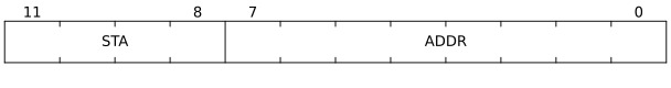
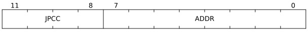
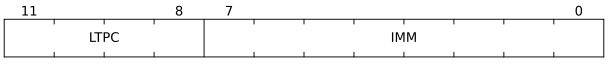
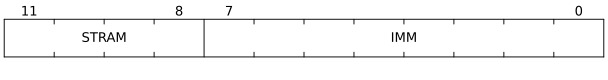
Every instruction is 12 bits wide and there is a maximum of 16 instructions, they all follow the following format:

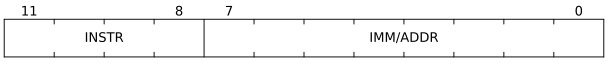
With a maximum of 16 instructions, 4 bits are needed to select the instruction. The other 8 form an immediate value or an address for the RAM.
To keep everything simple, the CPU has 1 usable register, called the ACC register. As it can directly read and write to 256 RAM bytes, those are used as a kind of registers in the way a normal RISC CPU uses registers.
The StupidCPU also has 2 status bits, carry and zero. Carry is high when an overflow occurs and zero when the ACC register is zero.
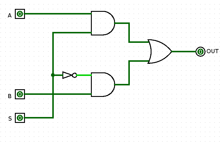
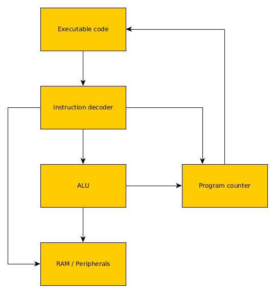
The high level architecture looks like this:

Instructions:

At the moment the instruction set is as follows:

NOR:
The NOR instruction executes a logic NOR on the ACC and the RAM value at the selected address, the result is stored in ACC.
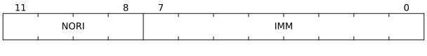
NORI:
The NORI instruction executes a logic NOR on the ACC and the immediate value, the result is stored in ACC.
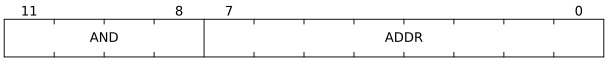
AND:
The AND instruction executes a logic AND on the ACC and the RAM value at the selected address, the result is stored in ACC.

ANDI:
The ANDI instruction executes a logic AND on the ACC and the immediate value, the result is stored in ACC.

ADD:
The ADD instruction adds ACC and the RAM value at the selected address, the result is stored in ACC.
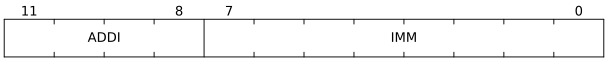
ADDI:
The ADDI instruction adds ACC and the immediate value, the result is stored in ACC.
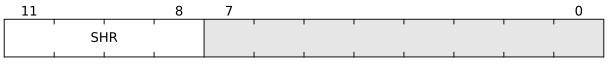
SHR
Logical shift ACC right 1 bit, store the result in ACC.
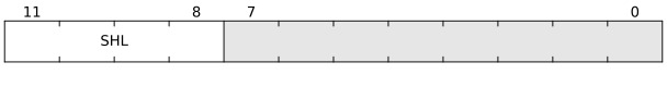
SHL
Logical shift ACC left 1 bit, store the result in ACC.

STA:
Store the ACC into RAM at the selected address.

JCC:
If carry is 0 or zero is 1, set the program counters lowest 8 bits to the immediate value.

JPCC:
If carry is 0 or zero is 1, set the program counter lowest 8 bits to the value in RAM at the selected address.

LPC:
Set the program counters lowest 8 bits to the immediate value

LTPC:
Set the program counters highest 8 bits to the immediate value, the next time the lowest 8 bits are changed. This means that after executing the LTPC instruction, the PC changed the next time an LPC instruction or a JCC/JPCC instruction with the carry at 0 or zero flag at 1 is executed.

STRAM:
Select the top RAM bank to use

This brings the total to 14 instructions out of the maximum of 16, so there is a bit of space left.
As this is a very limited set, some common macro’s are available, the assembler will translate them to the correct machine code:

NOP:
No operation.
Implementation:
Addi 0

NOT:
Invert ACC.
Implementation:
NORI 0

SUB:
Subtract ACC from the RAM value at the selected address, the result is stored in ACC.
Implementation:
NOT
ADD memaddr
ANDI 255
ADDI 1

SUBI:
Subtract ACC from the immediate value, the result is stored in ACC.
Implementation:
NOT
ADDI immediate
ANDI 255
ADDI 1

CLR:
Clear ACC
Implementation:
NORI 255

LDA:
Load an immediate value into ACC.
Implementation:
CLR
ADDI immediate

LDM:
Load a value from RAM into ACC.
Implementation:
CLR
ADD memaddr

MOVE:
Move a value from RAM to a different place in RAM
Implementation:
CLR
ADD srcaddr
STA destaddr

STORE:
Store an immediate value to RAM
Implementation:
CLR
ADDI immediate
STA destaddr

RAM banks:

The way the RAM works required some extra explanation, as it’s a bit unusual.
As the StupidCPU is an 8 bit CPU, it can access a maximum of 256 bytes of RAM, which is a bit low. To give it access to more RAM, bank switching is used.
With bank switching there are multiple banks of RAM, for example 4 banks of 256 bytes of RAM. The CPU can access one bank at a time, being able to select the accessible bank using a special instruction.

There is one problem for the StupidCPU, it has only 1 register. When the bank is switched, all previously accessible variables are gone. To counteract this, the StupicCPU has banks of 128 bytes, and only the highest 128 bytes of RAM are switched.
This way, the lowest 128 bytes of RAM are always accessible, the only downside is that with an 16 bit RAM bus the maximum amount of accessible RAM is 32K.

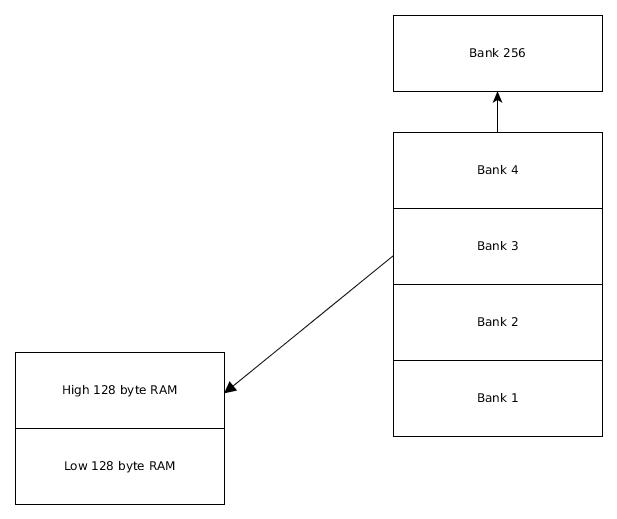
All peripherals are memory mapped, for example, an GPIO peripheral would be selected as a top bank and can then be written to/read from like RAM.


That’s it for now, the next blog post will go into some more design details.

Credit where credit is due:

The images made for the instructions where made with bitfield and the other images with yEd


A 7400 frequency counter, on perfboard

I like perfboard, especially the ones with plated trough holes. But I also like SMD components, and more and more fun IC’s are not available in DIP.  So a while ago I designed some perfboard with 1.27mm pitch, making some SMD parts like SOIC stuff easy to prototype on it, and also mix THT and SMD stuff.

Looking for a nice little project to build on it, I came across a frequency counter made with 7400 logic, perhaps not the most efficient approach, but a fun one at that. I made a few changed to the design, partly because of some components I already had like the 74HC160 and 4543 (yes, not 7400 but still logic :P) and partly to improve on the design, for example by adding a 10Mhz oscillator instead of a NE555 as the clock source. The current end result looks like this, a case is ordered and a follow up post will be made when the project is nicely tucked away in a case.

Continue Reading


Russian nixie, VFD and numitron overview

A lot of nixie tubes have been made in Russia, or more accurate, the USSR. These are still fairly easy to find and in some cases, quite affordable and just a few euro’s per nixie. Sadly I couldn’t find a nice overview of all the nixies made by the USSR. Some other popular displays are the VFD and numitron displays, both are also vacuum glass tubes and also used for DIY clock projects. This page will try to be a complete overview of all the nixie, VFD and numitron tubes in the popular IN and IV series.

Continue Reading


YASSD: chainable, UART controlled, 7 segment displays

For a few projects I like to use 7 segment displays to indicate a value like voltage, current or temperature. 7 segment displays are cheap, easy to read and easy to control. The biggest downside is that it can cost a lot of IO pins on a microcontroller to control a handful of 7 segment displays. One option is to buy finished 7 segment displays on Ebay that can read in a voltage. The downside of these is that the accuracy is not great and they can only be used if a certain range in voltage is what you want to display.

So time to design my own, yet another seven segment display, or YASSD for short. They have a 4 digit 7 segment display on one side and a STM32F031 and a 74HC595 on the other. Other features are:

  • UART controlled
  • Maximum of 8 on one UART bus, 3 solder bridges determine the ID of the display
  • Software updatable via UART
  • Easy to mount on a frontpanel

They look like this:

The hardware is simple, an ARM M0 microcontroller translates the UART messages to data for the 74HC595, some NPN transistors are used to select the digit. The reason for the, somewhat overkill, STM32F031 ARM M0 microcontroller is that it’s cheap, with a bit more then 1 euro per IC, it contains a UART bootloader, so other people that want to build this display only need a PC with a USB to UART converter and that it’s a microcontroller I’ve used often before. There is one bodge wire, I forgot to connect the GND from the 3.3V regulator to the rest of the PCB. In the files uploaded on my github this is fixed.

The 8 resistors of 100 Ohm close to the 74HC595 limit the current for the display. With the red 7 segment display used the current is a bit less then 10mA per segment, but these need to be recalculated for a different color display and on how bright the display has to be.

Controlling them is easy, connect them to a PC or microcontoller, setup UART to use a 19200 baudrate and send a string formatted like this: “ID,VALUE\n”. For example: “07,1234\n” would make it display 1234 if the YASSD has 7 as it’s ID. Adding a dot is no problem: “07,20.01” will display 20.01.

The ID is determined via the 3 solder bridges using the following formula: ID = (SB1 * 1) + (SB2 * 2) + (SB3 * 4). If a solder bridge is not present, SB is 1, if the bridge is present, SB is 0. This means that if there are no solder bridges present, the ID of the board is 7. By having YASSD’s with a different ID it is possible to connect a maximum of 8 on one UART bus.

The hardware and software are both open source and can be found on my github.


Abusing DMA for fun and LEDs

This blog post assumes you know the basics of multiplexing and how an LED matrix works. The end result looks like this:

Let’s say you want to control an LED matrix. A plain boring 8*8 LED matrix you bought on Ebay a long time ago and is still somewhere in your desk. It’s pretty simple, after figuring out how multiplexing works you’ll have a smiley drawn on the LED matrix in no time at all. But it’s much prettier if the brightness of an LED matrix can be controlled via PWM, maybe make some nice animations as well. For an 8*8 LED matrix, 8 PWM outputs would be needed and you are good to go, something a bigger microcontroller generally has available. But what if you want a bigger LED matrix, 16*16 perhaps. And animations running smoothly at a high frame rate.

For an 8*8 LED matrix, to make it look smoothly, you need to multiplex the screen at about 100 Hertz minimum. So set a column, wait a short time, switch to the next column and set the value for this column, wait a short time etc etc. With 100Hz there is 10ms of time per screen, so about 1.2ms (10ms / 8 columns) per column. More then plenty to set some IO pins to show an image. For a 16*16 LED matrix this time halves to 0.6ms. PWM makes this a bit harder, as a whole PWM cycle must fit in this 1.2 or 0.6ms, meaning the PWM peripheral must run at 833 or 1666Hz minimum. This is all no problem for a PWM peripheral in a modern microcontroller.

But what if you don’t have 8 or 16 PWM pins? For example, an Arduino Mega has 12 PWM pins. ARM M microcontrollers like the STM32F103 have more PWM pins, but those are shared with other peripherals as well, so they might not all be available to use in a project.

An option is to bitbang PWM, toggle an IO pin quick enough to act as an PWM pin. This has the major downside of costing a massive number of CPU cycles. To get just 6 bit PWM, so 64 different levels of brightness, in the 0.6ms for an 16*16 LED matrix, the CPU must check 64 times if that IO has to be set high or not. This means that every ~10us the CPU has to handle IO. If you also want to calculate some animation to display, the CPU will be very busy.

This is where the DMA comes in. The DMA, or Direct Memory Access, is a peripheral available in many modern microcontrollers. Simply said, it’s a co-processor that can copy data from one place in the microcontroller to a different place without the CPU having to do a thing. It can be used to transfer an ADC value to a buffer in RAM and give a sign to the CPU when the buffer is full. The microcontroller I’ve used for this blog, the STM32F103, can transfer memory to memory, peripheral to memory and memory to a peripheral without the CPU doing a thing apart from setting up the DMA. Transferring data to a peripheral without costing CPU cycles. That sounds like a nice way of driving an LED matrix.

Continue Reading


Numican, a small numitron clock

I wanted a numitron clock on my desk. As, in my opinion, a decent looking enclosure is one of the hardest things to make I made the clock in the size of an altoids can so just a few holes should be made for an enclosure that looks not too ugly. It’s almost fully in SMD and can be powered using a USB port, making it a lovely clock for almost every desk.

In the end I ordered a custom enclosure from Schaeffer in Germany for a nicer looking clock.

The build process, design files and such can be found on hackaday.io as I used the project to try out hackaday io and see if it worked for me.The link is: https://hackaday.io/project/18166-numican


Quick GUI for MBED projects, part 2

The previous post I explained the code for the dear ImGui part of the GUI. In this part the code for the serial connection will be discussed.

This code is made up of 2 parts, the MBED code and the PC side code. The MBED code will be discussed first. The MBED code uses the excellent MODSERIAL library. The MBED code after stripping away the initialization and such looks like this:

Continue Reading


Quick GUI for MBED projects using Dear ImGui and Serial

A lot of microcontroller projects communicate with a computer using a serial connection as this is still a very simple and cheap way of communicating. Making a program on the PC to communicate with a microcontroller can however be a bit tricky. On accident I stumbled on the Dear ImGui library, a C++ library to quickly make a GUI, for debugging a C++ project for example. I really liked the look of it, it looked really simple, with a lot of usable gui objects. Dear ImGui can use OpenGL, DirectX, Vulcan and more. It is cross platform as well, as long as OpenGL is used.

A gui is just half of the issues solved, a good library for serial communication is also needed. After a quick look Serial popped up. Except for the annoyingly generic name it is a very nice looking library. Cross platform and simple to use, being made to look and feel like PySerial.

With these two libraries it is possible to make a C++ cross platform GUI for all kinds of microcontroller projects. I decided to make a simple project first that can read and write to some IO ports, set the DAC and read in two ADC’s.

And the result looks like this:

Selection_009

Continue Reading


Ebay headphone amplifier kit

A while ago I bought the following headphone amp on Ebay as it looked like a nice small project. The included case and battery are also quite nice and the price was very affordable. A few weeks later the parts arrived in a very recognizable china envelope. In the package I found, exactly as pictured on Ebay, A nice looking PCB, a bunch of parts, a battery and a case. The first downside is the lack of documentation. There are no build instructions, making it a bit less nice for beginners.

All the values of the parts are printed on the PCB silkscreen and written on the parts whenever needed. So building it takes a bit of figuring out but is very doable. 2 issues arise fairly quickly though. The diodes have no anode or cathode marked on the PCB and the IC that is surrounded with diodes has the marking removed. I think it’s clear where this is going, I soldered all three diodes incorrectly and after correcting the IC got insanely hot in less then a second. Lovely.

WP_20160123_15_48_37_Raw_LI WP_20160123_15_09_23_Raw_LI

The rest of the PCB went OK to build, the parts are from a good quality brand and the PCB looks nice with the gold plating on it. The only issue where the diodes.

WP_20160124_13_20_41_Raw_LI

But now I’m stuck with a non working PCB as the IC that generates the voltages for the opamps is well, dead. After emailing the seller they couldn’t give me the schematic. So well, time to reverse engineer the schematic :)

Continue Reading


Pages:12345