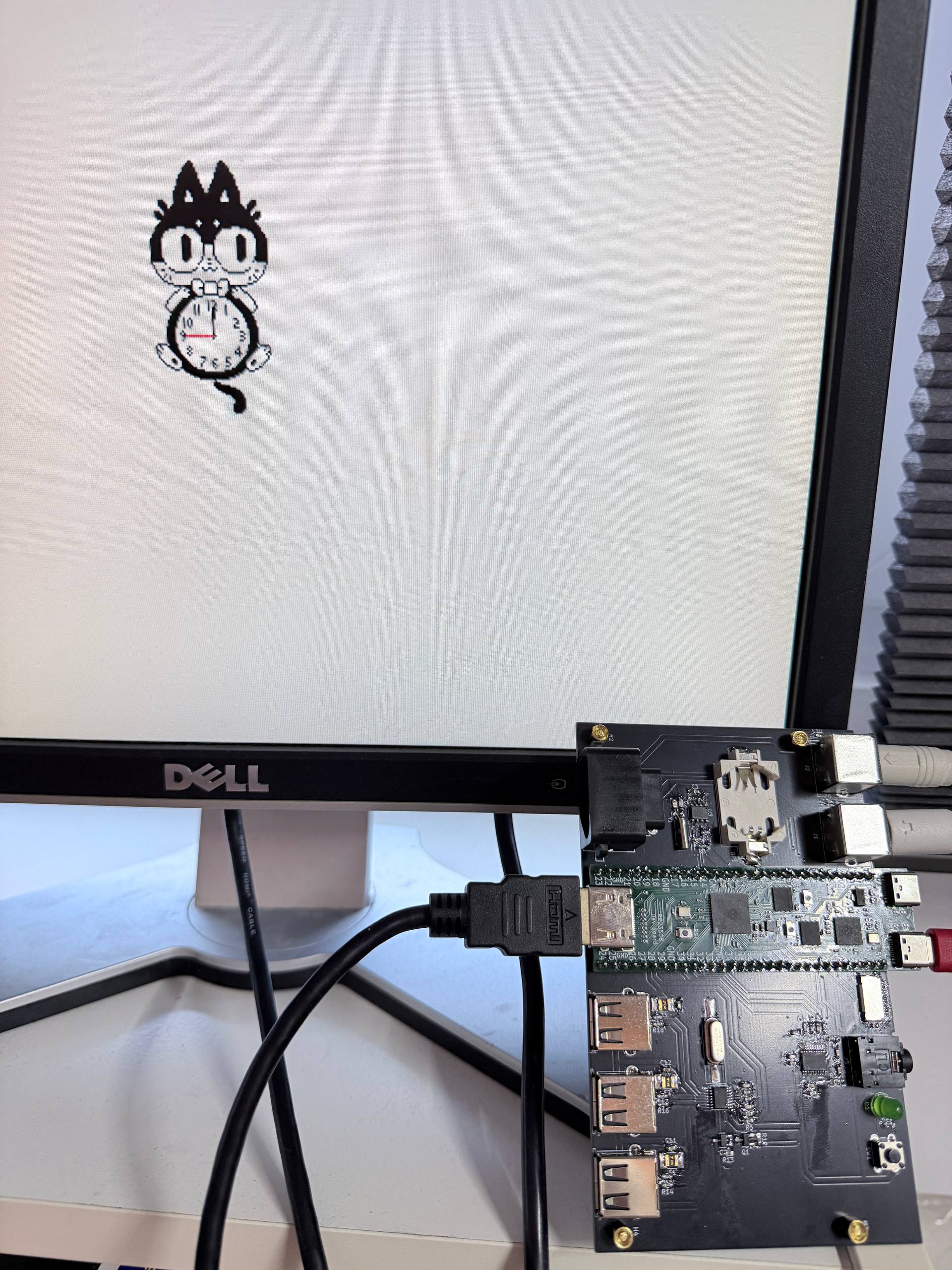
What’s a “Varvara” and why does that pi pico 2 look a little different? Let’s dive into that!
Varvara is a specification for a computer system, which uses the Uxn virtual machine and describes how things like a display, mouse, keyboard and such should react. Uxn, in term, is a spec for a virtual machine or virtual CPU. It’s a stack based 8 bit CPU that is meant to be easy to learn and emulate.
It’s essentially a graphical computer specification! The goal is to have an easy to implement and emulate computer with it’s own programming language, so programs can be written once and run on everything. And the computer is made to be easy to program for, as all the devices like files, screen and such are very abstract.
For example, there is no notion of a file system. There are just commands to read, write and delete files. The emulator handles the rest. For the display, to draw a sprite, the address of the sprite is placed in the right location and then a command is issued to draw it.
This feels very much like an 8 bit home computer done right, not having to care too much about hardware limitations of that era. There is also a ton of programs and guides for it, from small tools like a calendar and notepad to quite some games. There is also a great tutorial on programming for the Varvara computer here which I highly recommend to check out!
Of course, my brain went: Huh. can I run this on a micro-controller?
So I tried in the past using a Pi Pico, but it just wasn’t meant to be. The Pi Pico 1 felt just a bit too small and limited. But then the Pi Pico 2 launched, with twice the RAM. So let’s try again :)
OK and make a custom RP2350 board because I got annoyed at the Pi Pico 2, can’t have a project without a little yak shaving!
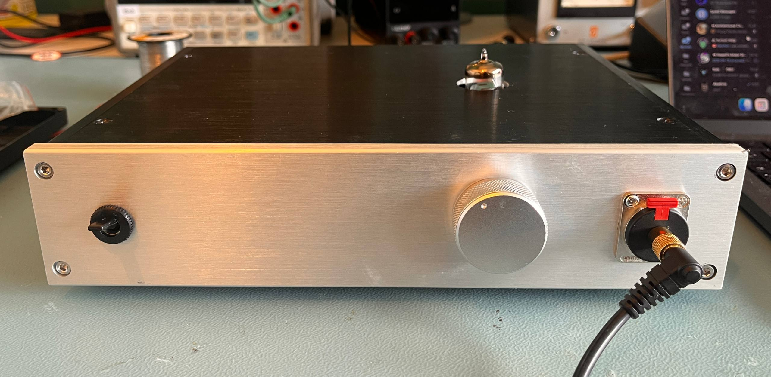
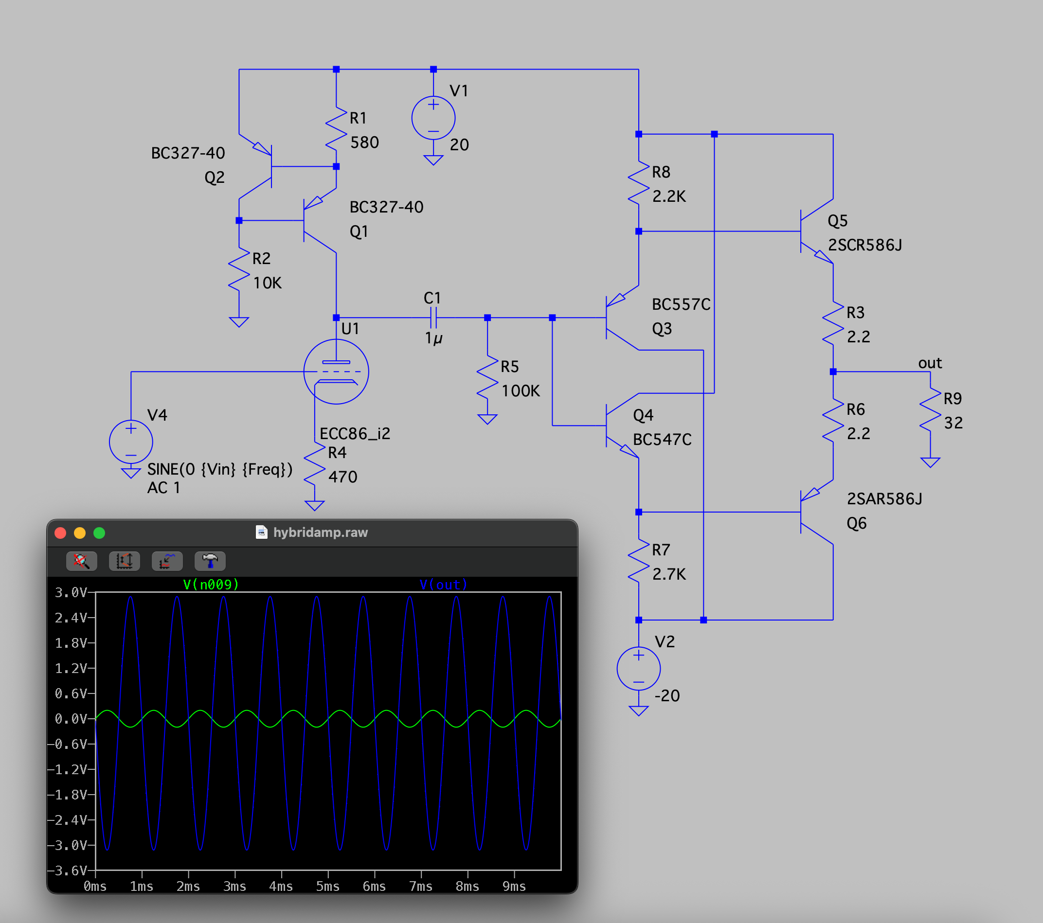
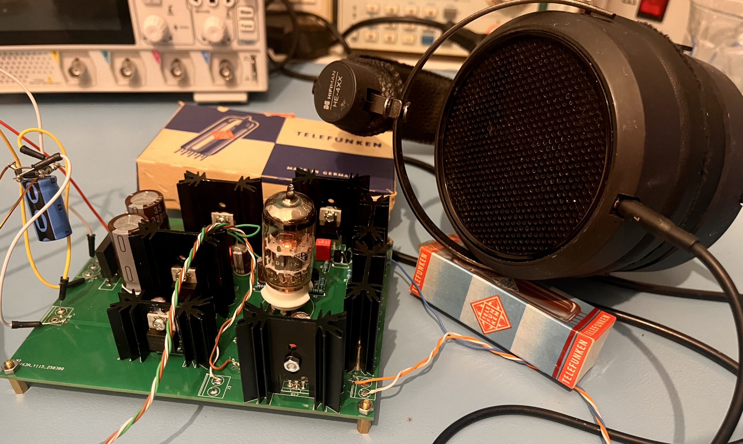
It’s been a while, but let’s finish that tube amp project and see why you should likely not build one yourself! But before we get into the details, a quick recap of the first part. The amplifier is a hybrid amplifier using a ECC86 as voltage gain stage, combined with a transistor buffer to drive headphones. The interesting part of designing and testing the amplifier where done, so now onto the boring part, iterating and building a finished product.
This repair has been on the to do list for ages, so let’s finally get to it!
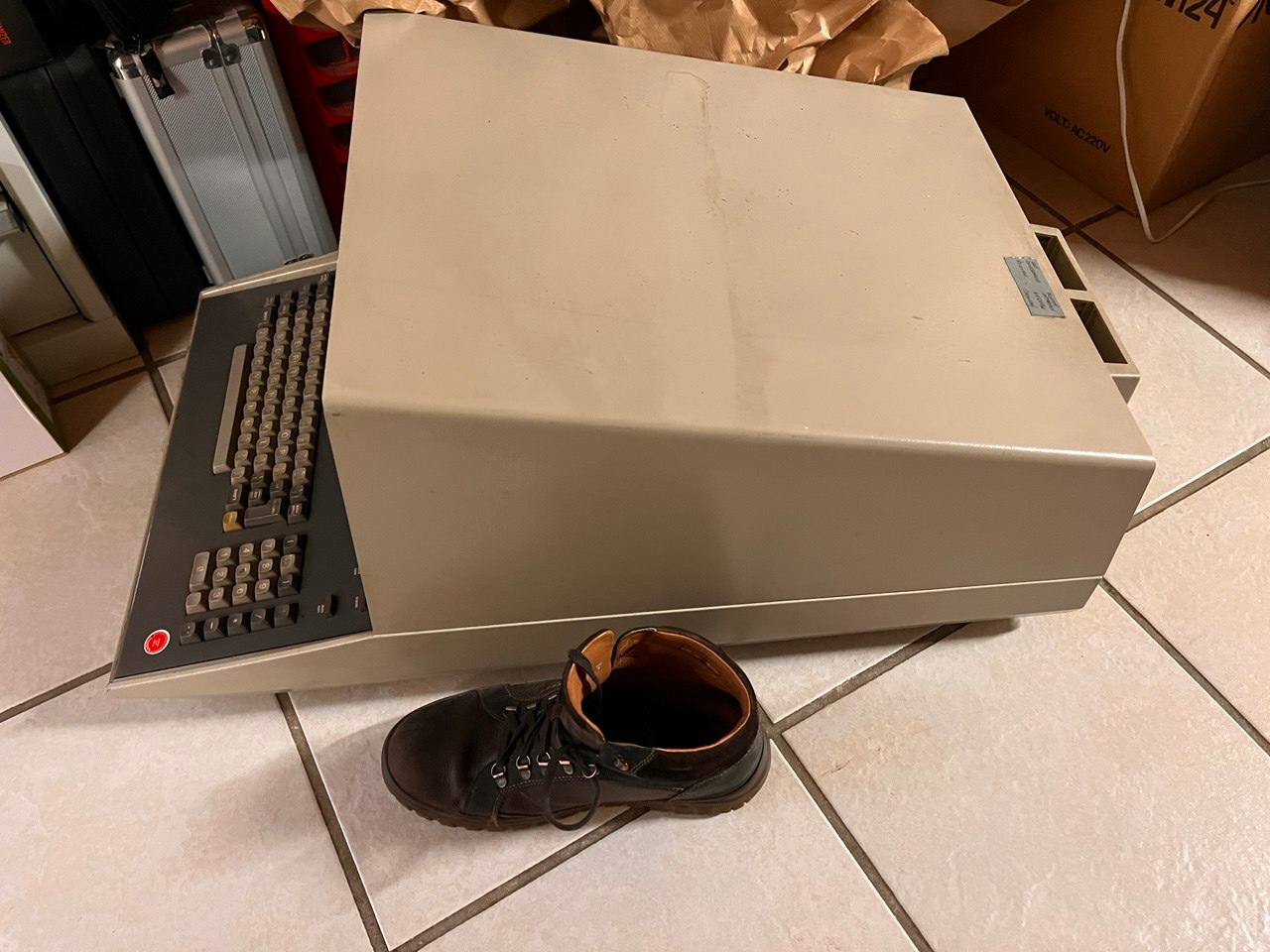
In my mind, Tektronix is a brand that makes electronics lab equipment like oscilloscopes and logic analyzers. Turns out, they made quite a few terminals and a couple of computers! A good friend saw this one for sale local to him, and I poked him till he agreed on picking it up for me.
Picking it up may be the wrong wording, this thing is big and heavy! It weights about 35kg and it’s nearly a meter long!
So let’s have a look at what this is, what I needed to do to repair it and what it can do!
Some history
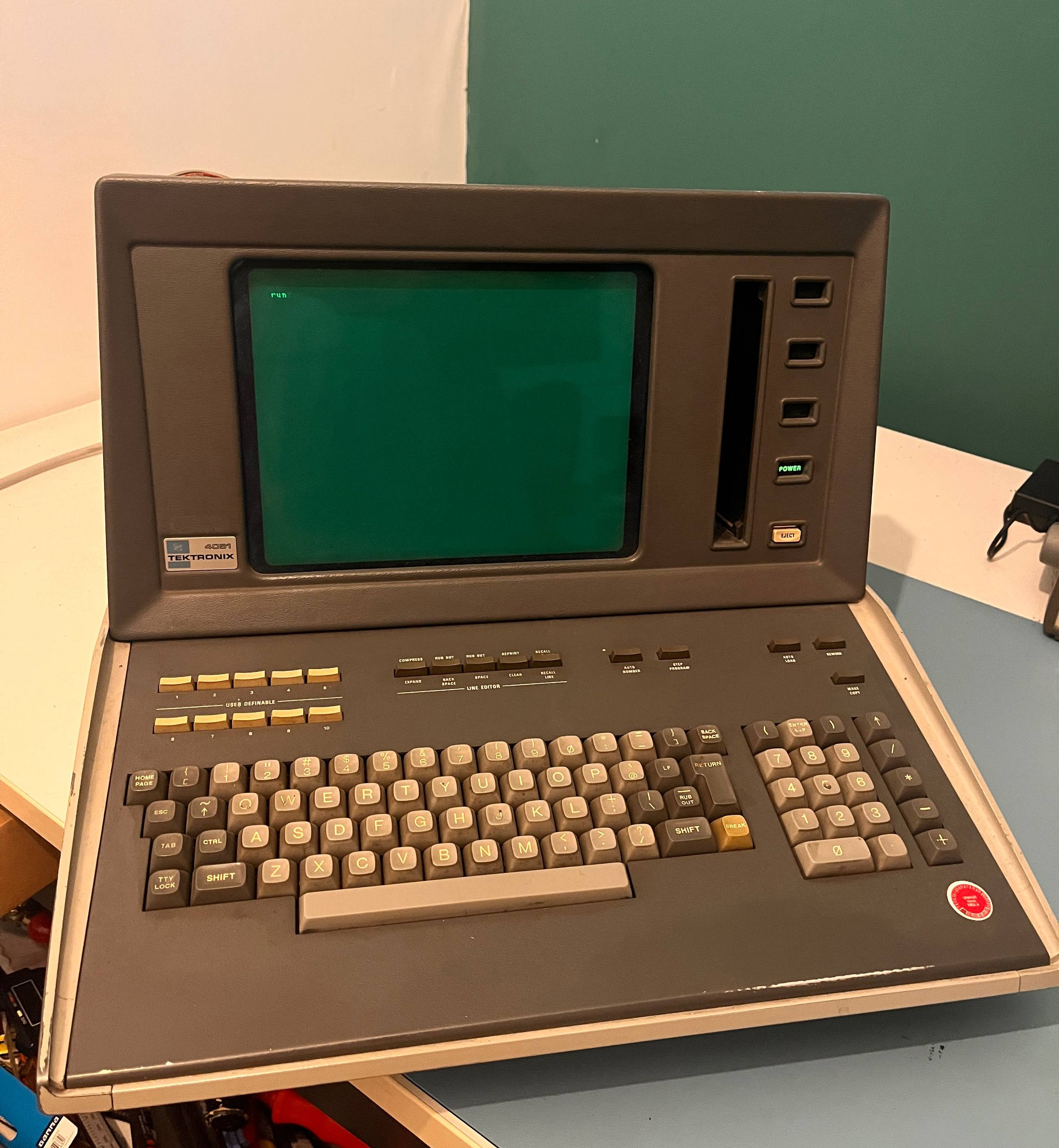
The machine I got is a Tektronix 4051 graphics workstation, released in 1975, but let’s look a bit at the history from Tektronix before this was released. Tektronix started in late 1945 as Tekrad, but quickly got renamed to Tektronix. One of their first products was the 511 oscilloscope, the first oscilloscope with a trigger!
This turned out to be a good thing, and soon enough, Tektronix was synonymous with oscilloscopes and known as a company that made some of the best test and measurement equipment. In the 60s, mainframe and then minicomputers became more popular, which often needed a terminal. Tektronix at this point was making storage oscilloscopes, which use a storage CRT tube that can “remember” drawn signals. Using this technology, Tektronix released their first terminal in 1969, the 4002. A 11″ terminal that was capable of displaying graphics with a 400×300 pixel resolution. As the CRT rememebers the drawn data, there was no need for a RAM framebuffer!
A few years later in 1971 they released the 4010, again 11″ but now with 1024*780 pixel resolution. As they used Storage CRTs, these terminals where a lot cheaper then the competitors. Mind you, cheap still means around $4000, or around $30.000 in 2025 money. But the IBM 2250 was priced at around $280.000 That’s 1970s dollars, so well over 2 million USD today!
Before we move away from these terminals, one last cool tidbit. Tektronix made the 4010 in several sizes, the biggest being the 25″ 4016 with a 4096*3120 pixel resolution. 4K in 1974, sign me up!
The 405x computers
OK I promised computers, so let’s move to the Tek 4051 I got! Released in 1975, this was based on the 4010 series of terminals, but with a Motorola 6800 computer inside. This machine ran, like so many at the time, BASIC, but with extra subroutines for drawing and manipulating vector graphics. 8KB RAM was standard, but up to 32KB RAM could be installed. Extra software was installed via ROM modules in the back, for example to add DSP routines. Data could be saved on tape, and via RS232 and GBIP external devices could be attached!
All in all, a pretty capable machine, especially in 1975. BASIC computers where getting common, but graphics was pretty new. According to Tektronix the 4051 was ideal for researches, analysts and physicians, and this could be yours for the low low price of 6 grand, or around $36.000 in 2025. I could not find sales figures, but it seems that this was a decently successful machine. Tektronix also made the 4052, with a faster CPU, and the 4054, a 19″ 4K resolution behemoth! Tektronix continued making workstations until the 90s but like almost all workstations of the era, x86/Linux eventually took over the entire workstation market.
The 4051 was also used in a few series/movies, the storage CRTs do not flicker when recorded like a normal CRT and as they run basic, getting something cool on screen was fairly easy to do! The best known example was Battlestar Galactica:
Fixing a Tektronix computer
With the history out of the way, what’s the shape of the one I got?
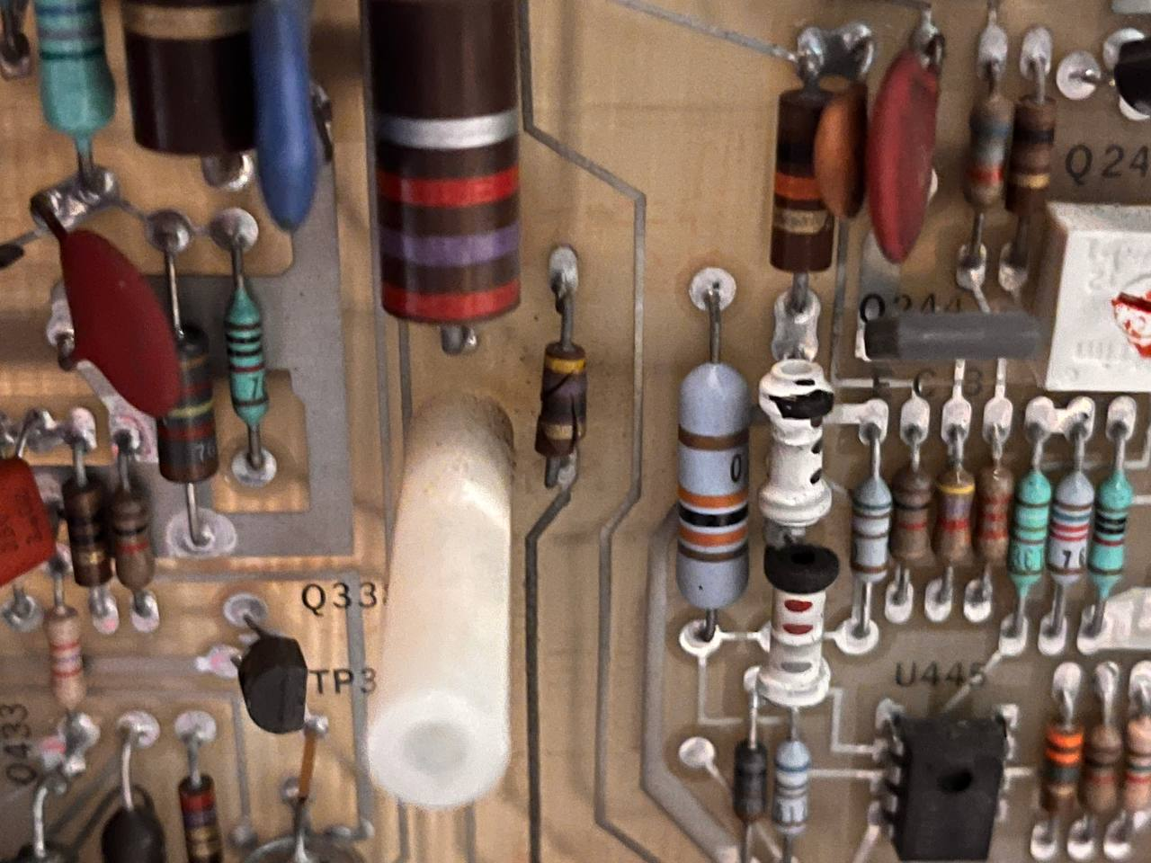
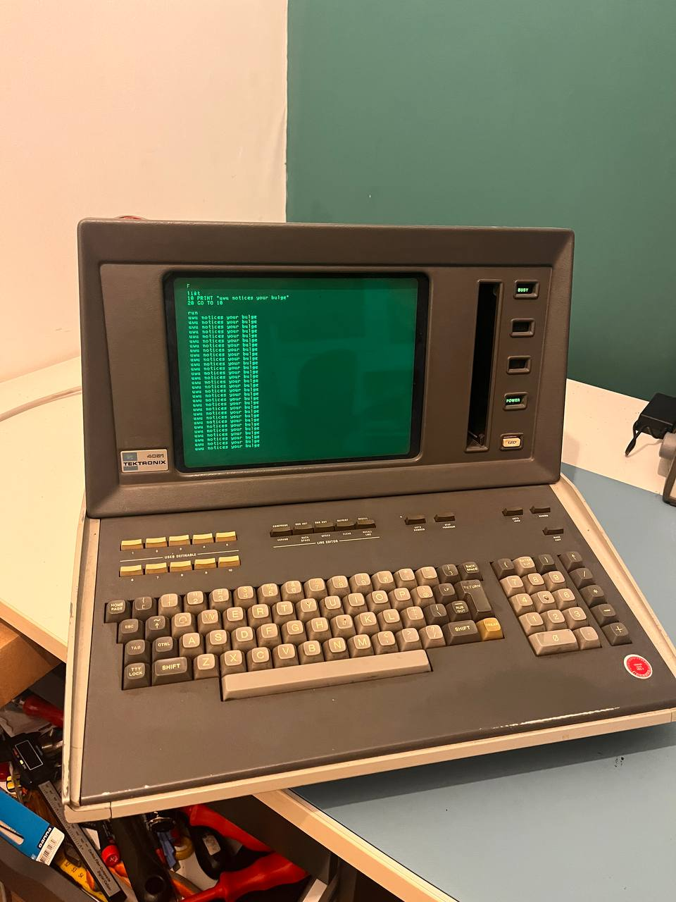
It was stored in a shed for a long while, state unknown, but it looked like it’s in OK shape. A bit dirty but who isn’t at times. Fuse is intact, and when opening it up, nothing looked “off” no bulging caps or such. But turning it on and nothing happens. Anticlimactic…
A good bit of tracing wires later, it turned out the ON/OFF switch is broken. So to quicly remedy this, some wires can be used.
I do NOT recommend this. 230V via cheap breadboard wires is not smart. But with this, still nothing. Argh. So another bit of debugging later it turned out a wire of the mains transformer was not connected to the terminal.
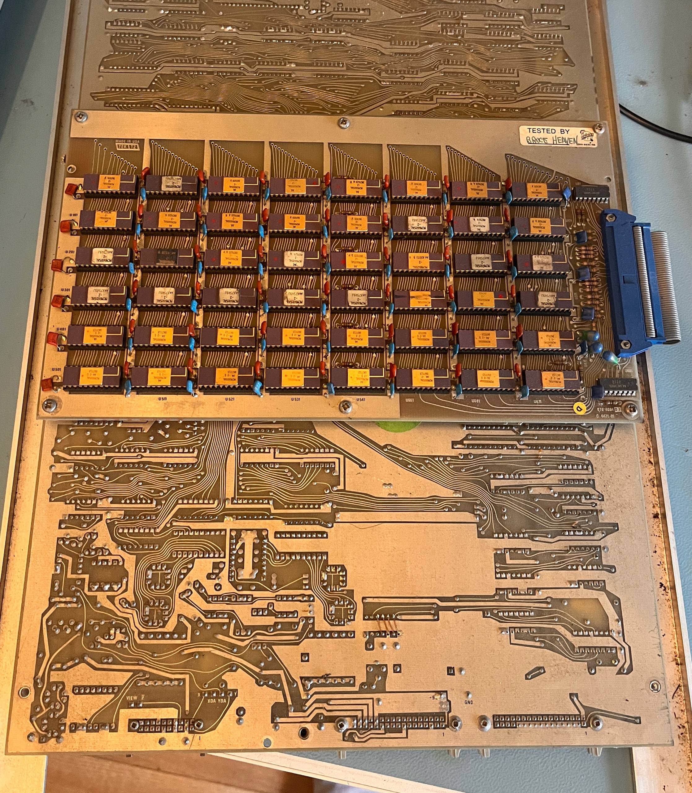
It’s kind of visible in this photo, there are wires going from the transformer to the tabs to select voltages and one was broken. Luckily there was enough wire left to solder on and fix it, getting a replacement would have been impossible! After this fix, I got power! I disconnected as much as I could in order to check all the voltages I could check. We need 15V, 12V, 5V, -12, +20, -20 +185 and +365 and they turned out to all be in spec. Tektronix :)
So, time to slowly connect boards back in and see if something explodes!
Wait I didn’t mean that as a suggestion… Sadly this resistor didn’t understand sarcasm and decided to go up in smoke. It’s a 47 ohm resistor that limits a 320V supply a bit. Perhaps it got a little too warm, or age got the better of it. I did check everything after the resistor and all measured OK. No transistor in a short or capacitor that imploded. So let’s just replace this and pray?
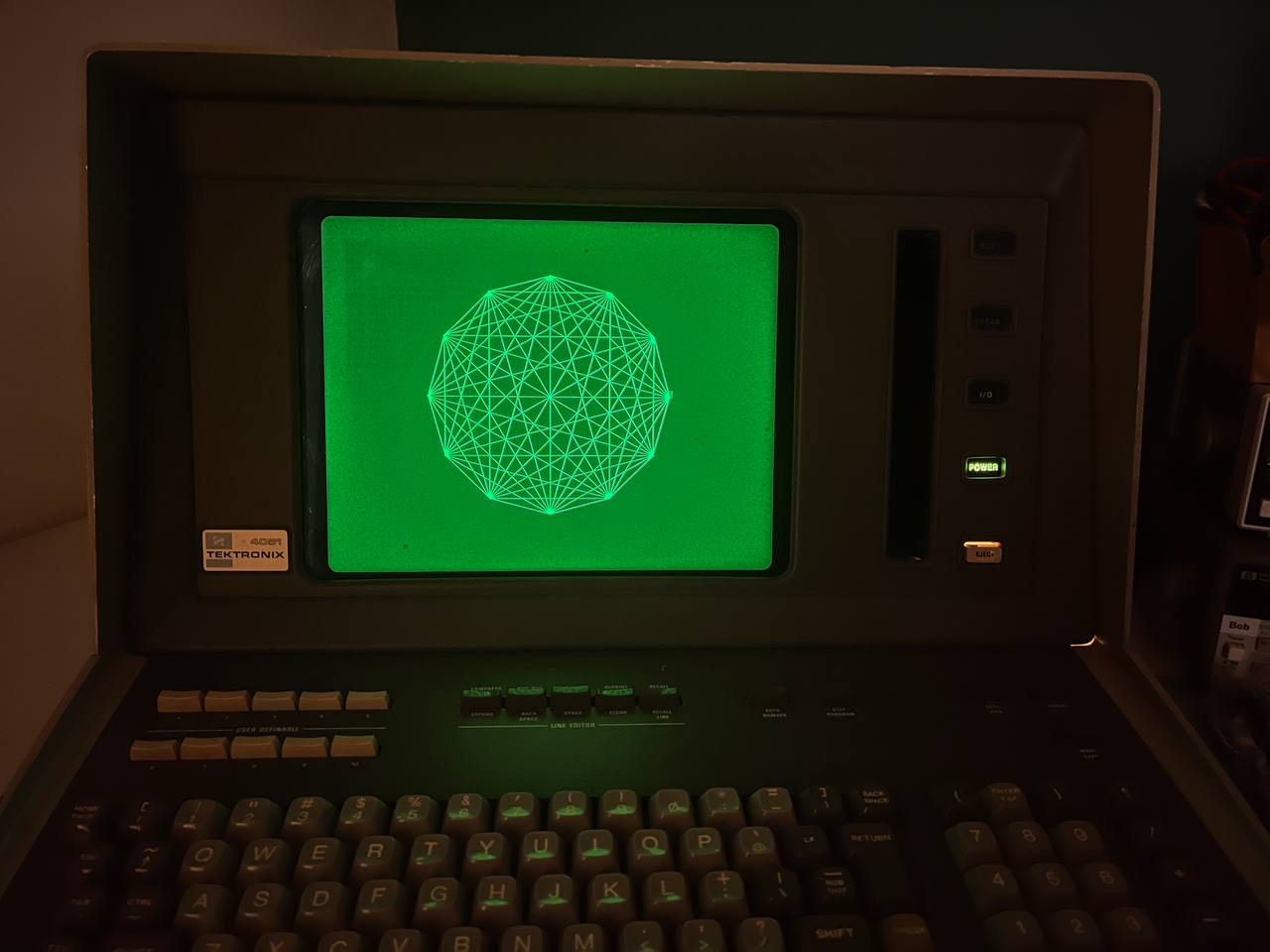
Neat, that worked!
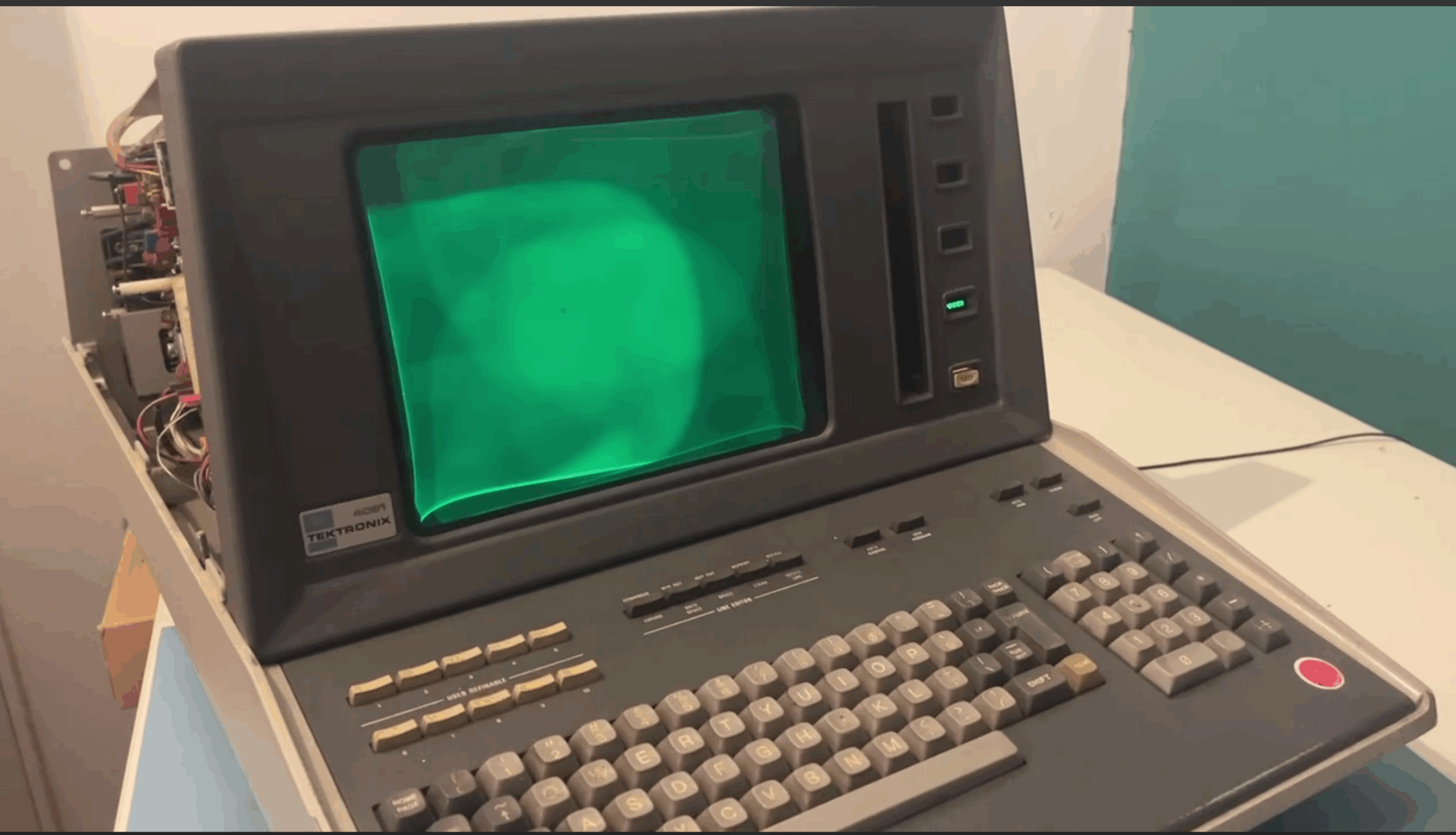
Calibrating that display
Something appeared on the display, which is a BIG improvement, and it all looks like the machine wants to boot. But the display is completely unreadable, which means it’s time to calibrate all voltages.
Which means, measure a power supply that’s almost 4KV. Spicy!
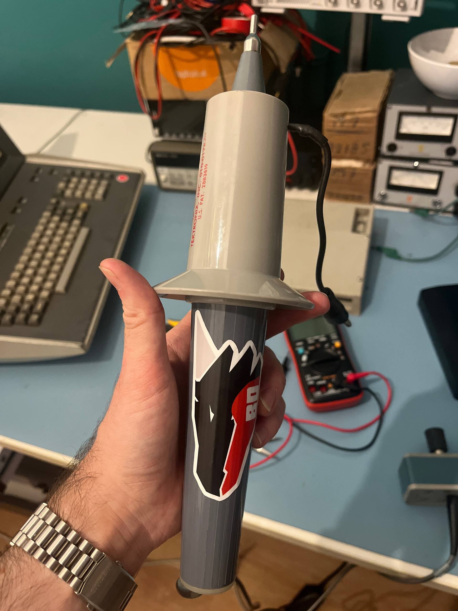
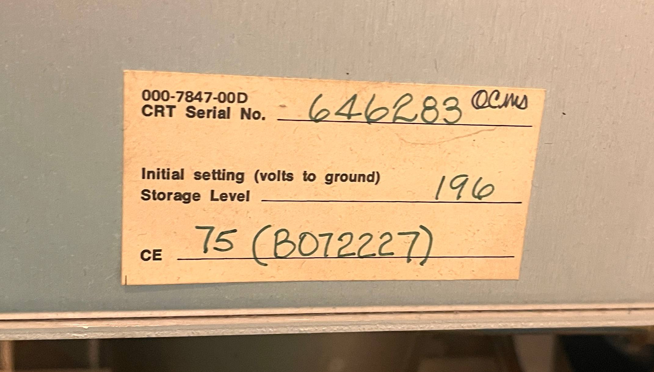
Luckily I have a HV scope probe on loan from a friend! And the HV is in spec. So that’s good, but all the other voltages are not. These CRTs are pretty sensitive to all the needed voltages, sensitive enough that they are calibrated in the factory and the voltages for the exact CRT are written on them:
196V and 75V for this one, and I measured 160V and 55V. yeah that’ll do it! Quite a few calibration steps later the display turned out to be quite nicely readable and in great condition!
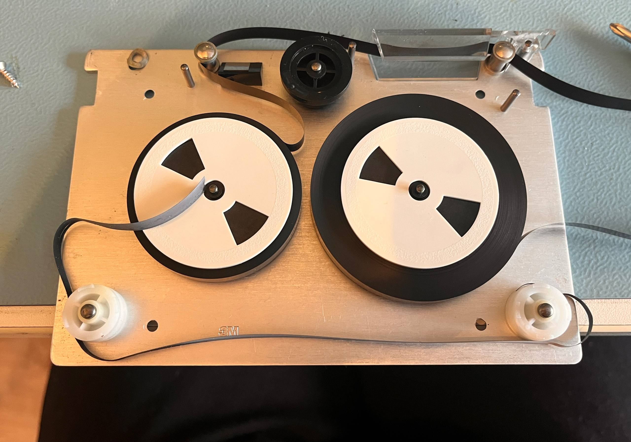
The single tape I got with mine is sadly broken. The belt snapped, which seems to be a common issue with these. The drive itself seems to work, and the tape I got is an OS backup tape, so likely nothing too important. This is fixable, but not too high on my to-do list for now.
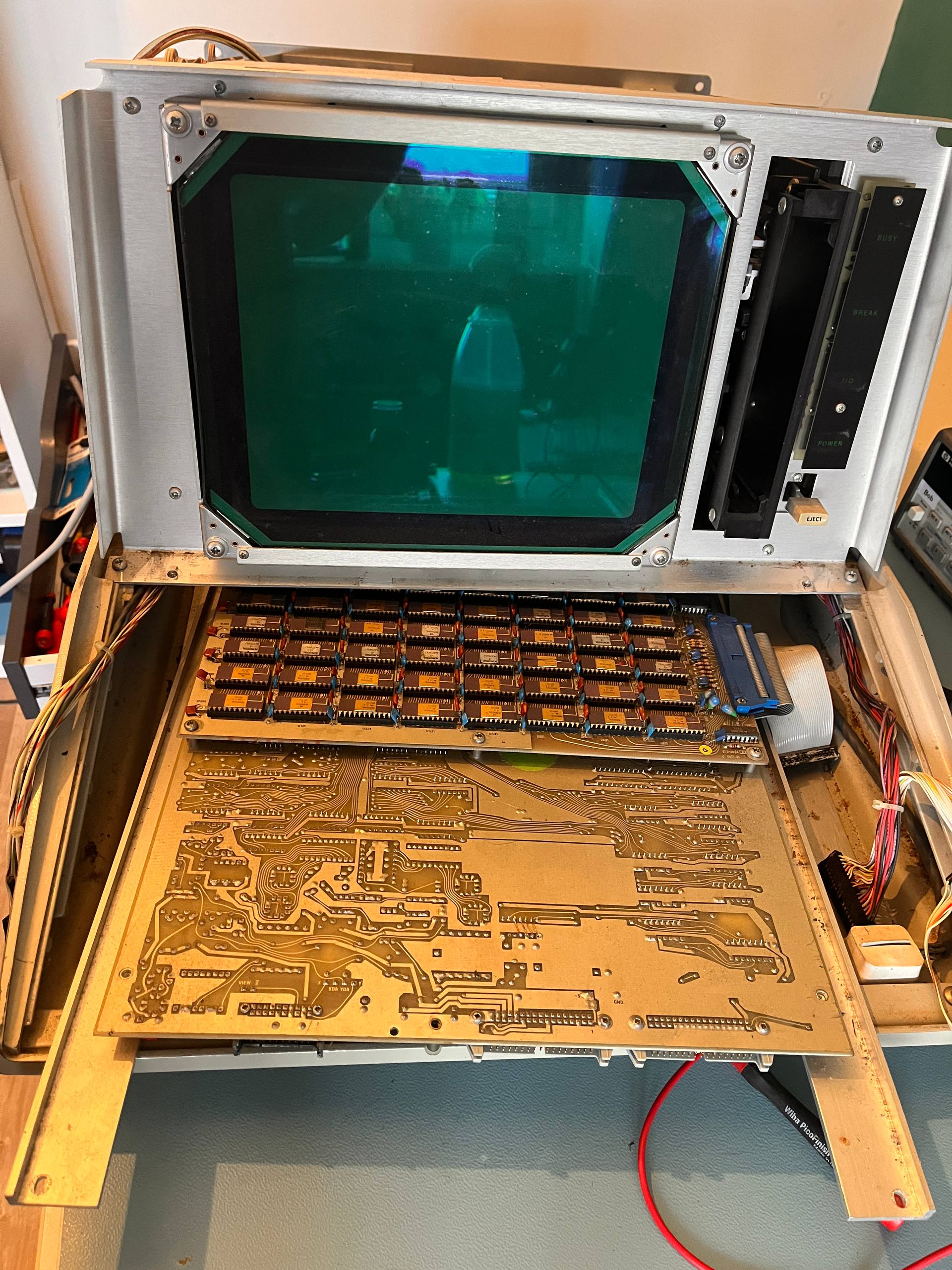
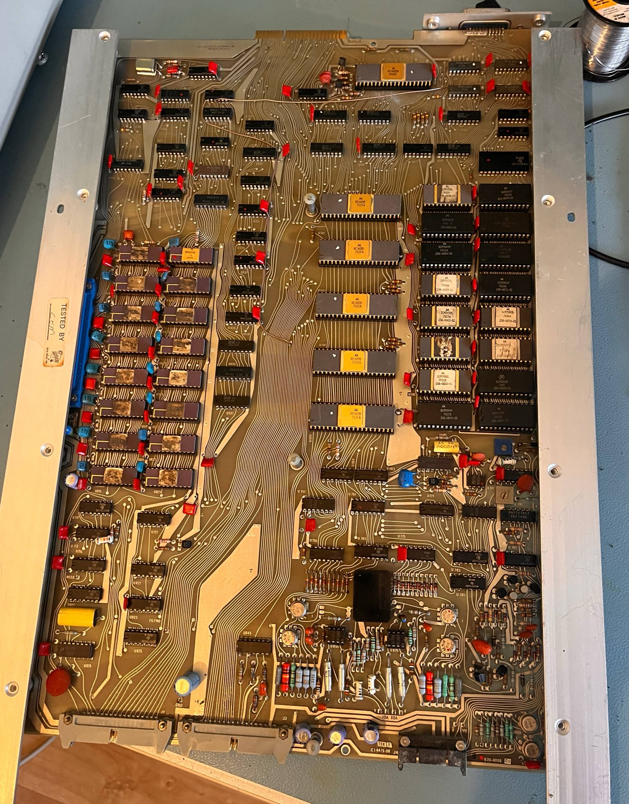
This turned out to be a less complex repair then expected. Some keyboard switches are a bit crusty, it needs a clean, but a 50 year old computer mostly just working is pretty amazing! So let’s end this repair on a few fun beauty shots of the inside and more:
What did I pick up exactly?
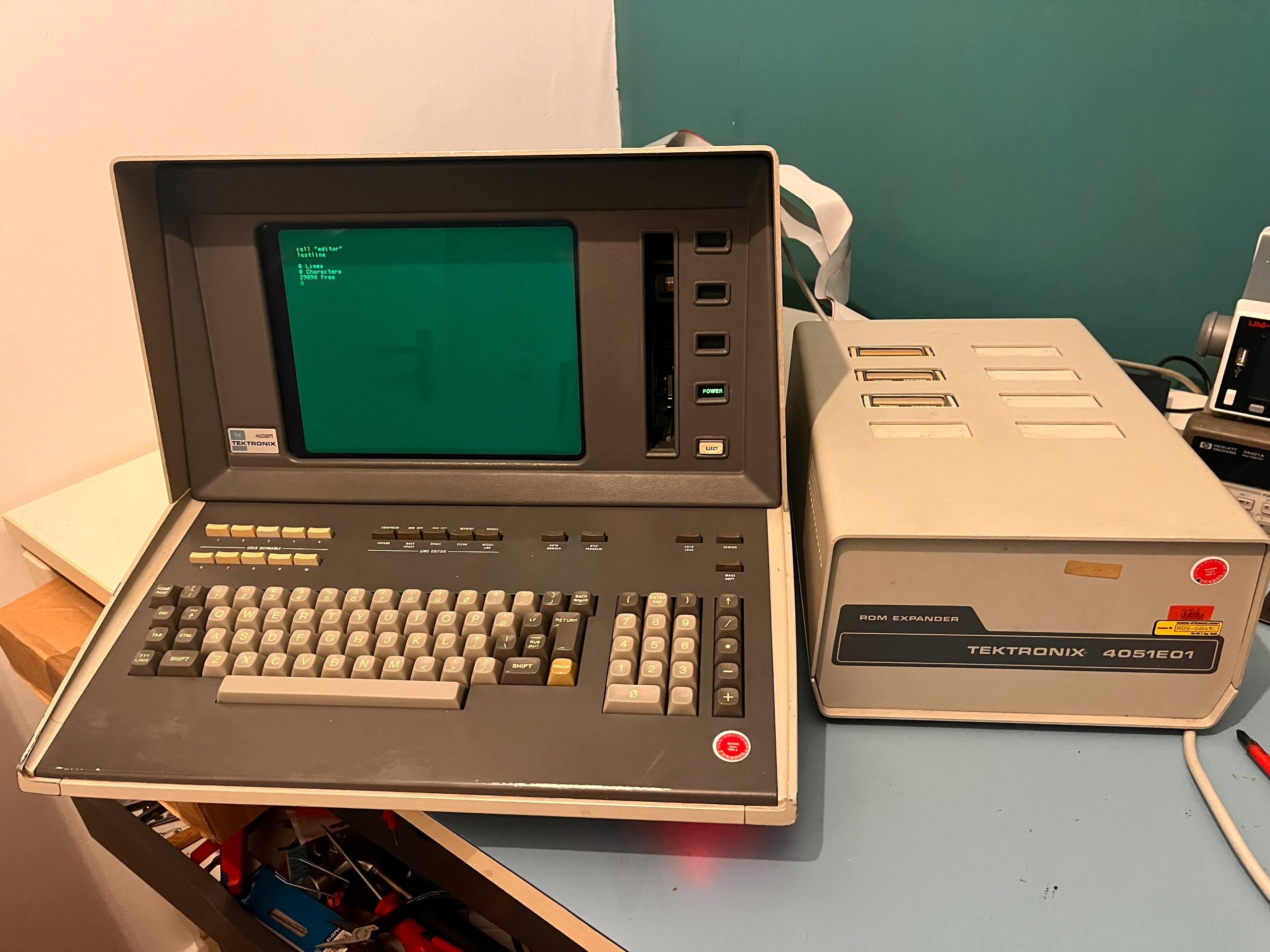
Having a look at my machine, it has maxed out RAM at 32KB, sadly no serial port, but it did came with a ROM Expander!
The back of the 4051 has space for 2 ROM cards. These contain things like extra programs, subroutines for DSP algorithms and more. These can contain 8KB of ROM, and are memory mapped.
If you want more then 2 at any time, the Rom Expander allows you to have 8! Only one is memory mapped at any time, but the OS of the 4051 scans all ROMS on start, and when you run a program on a ROM, it makes sure to send a few commands to the expander to memory map the right one. This is all invisible as an end user and the machine acts like having 8 ROMs, or if you have 2 expanders, 16 ROMs!
I got 3 ROMs with mine, one for an editor program, one to load/store binary data to tape, and one for the optional external floppy drive. Oh, yes, there is a floppy drive! Sadly I don’t have it, but if someone has one collecting dust, do let me know :)
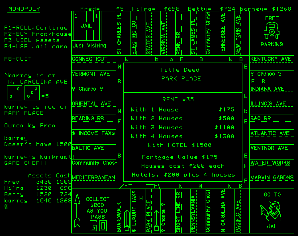
Due to the display technique, most games don’t work very well. The display can’t easily be cleared, apart from a full erase of the display. So some games like tic tac toe or monopoly work but anything more active is difficult sadly.
Luckily there are plenty of cool demo’s and programs for the 4051 and it’s bigger siblings. A TON of programs, manuals and more can be found on the Github page from Monty McGraw. There is also an emulator so you can try this all out using any modern computer!
What’s next
One of the projects on Monty’s Github is a GBIP flash emulator. Currently my 4051 has no way to load/store programs, and typing a 1000 line BASIC file is a bit of a pain. So I’m definitely ordering parts for that!
There is also quite a few ROM cards I do not have, so I am working on a ROM board to clone them.
Finally having this beautiful machine up and running is a great step, and I’ll leave it at this for now!
As always, if you enjoyed this blog post, you can buy me a coffee!
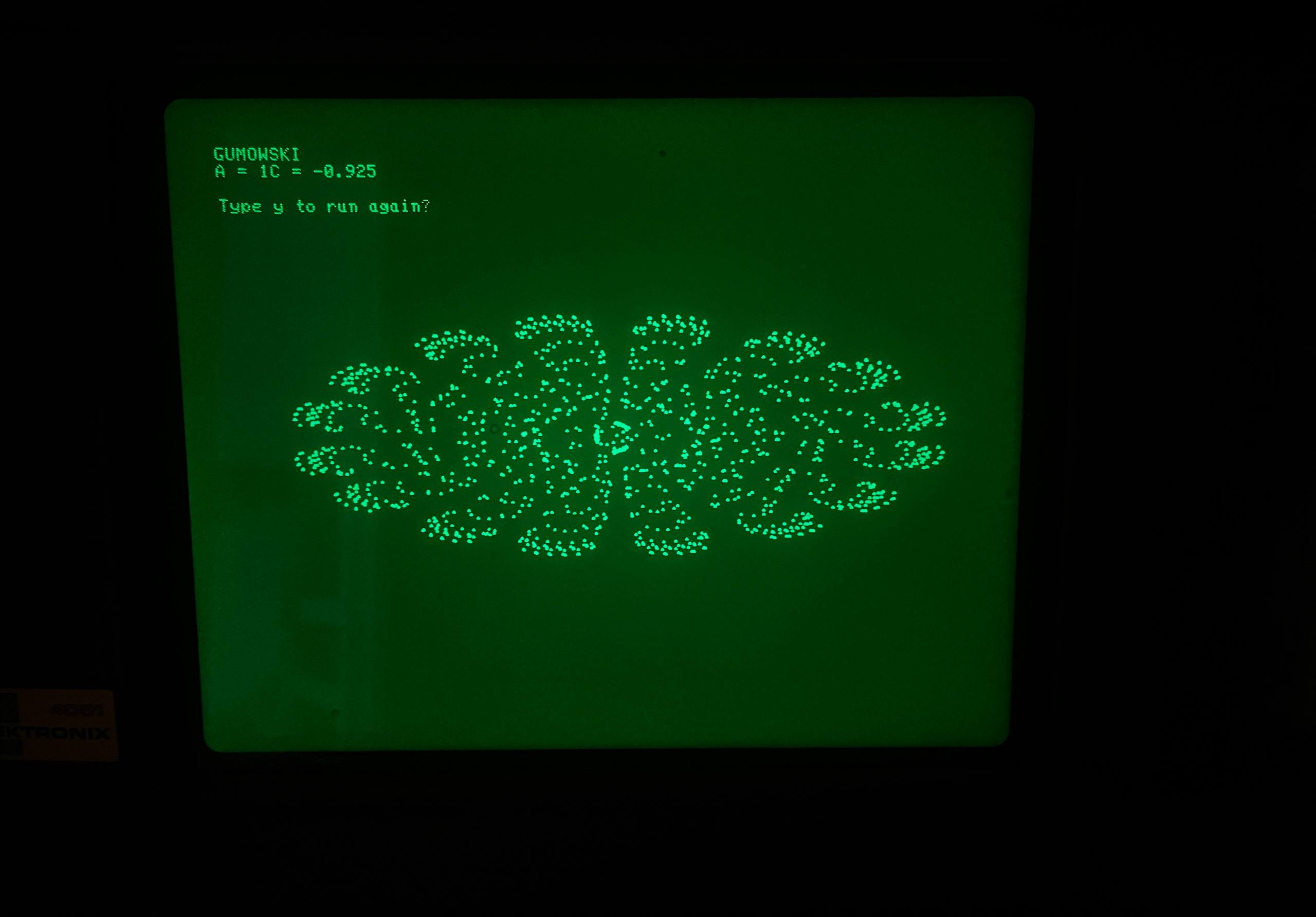
Gumowski from creative computing september 1987 page 88 https://archive.org/details/creativecomputing-1978-09
Do I need another headphone amp? Nah. Do I want to build one? Yeah! And this time one using a low voltage tube, the ECC86. So let’s dive into this fun little tube, some alternatives, and design a headphone amp around it. I will cheap out a bit and make a hybrid one though :)
So the idea is pretty simple, I wanted to make some tube amplifier that works on lower voltages. Which is something that most tubes don’t like to do. I had a few tubes in mind, one of them being the 28D7 as it needs 28V for both the anode and filament, one voltage for all is pretty handy! Another one is the 1S4, a single penthode that works on 45V and needs a super low 1.4V 100mA for the filament. This is so it can work on a 1.5V and a 45V battery. And the last one in mind is the more popular ECC86, a dual triode that works with just 12V or even less. In the end I went for the ECC86 as some popped up for sale recently, and the amplification factor seems to be about right for a headphone amp.
Now, none of these tubes (well maybe the 28D7 with a lot of shenanigans) can drive a headphone. Tubes all suck at delivering high currents apart from a few exceptions. So some current buffer is needed, this can be an opamp, some class A power stage or anything in between. I wanted to be able to drive about any headphone I could throw at it, and possible a speaker. So I wanted something with a good amount of oomph. This means most opamps are not going to cut it! I also didn’t want anything too complex so I decided to give a diamond buffer a try!
With all big chunks settled on, let’s try and design this thing!
Designing the tube section
To start, I tried out a very simple triode amplifier using the ECC86. An amazing guide on this can be found here, and if you are curious about designing tube amplifiers, It’s a highly recommended read!
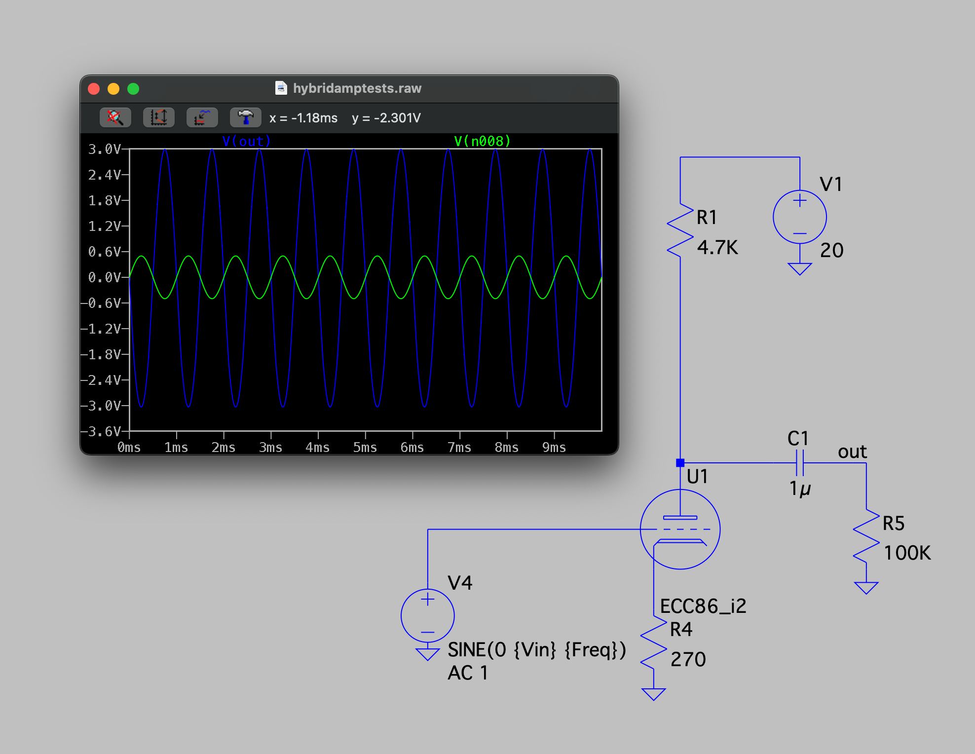
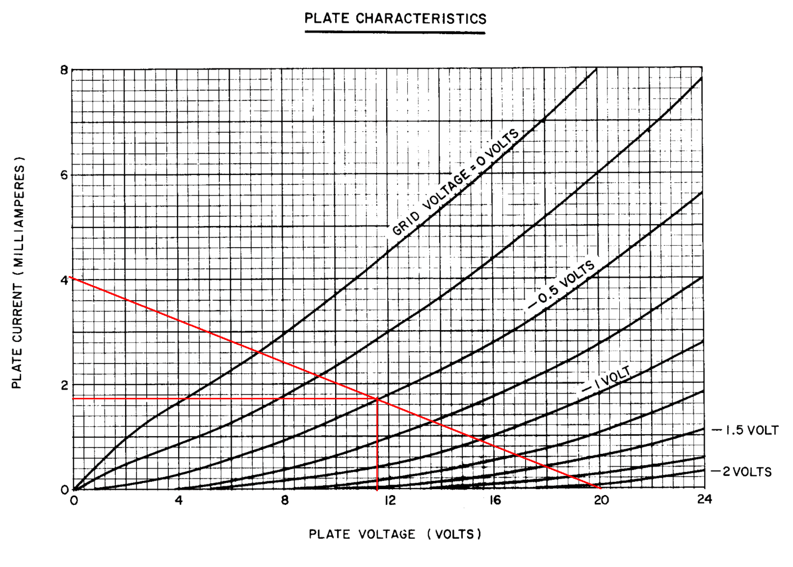
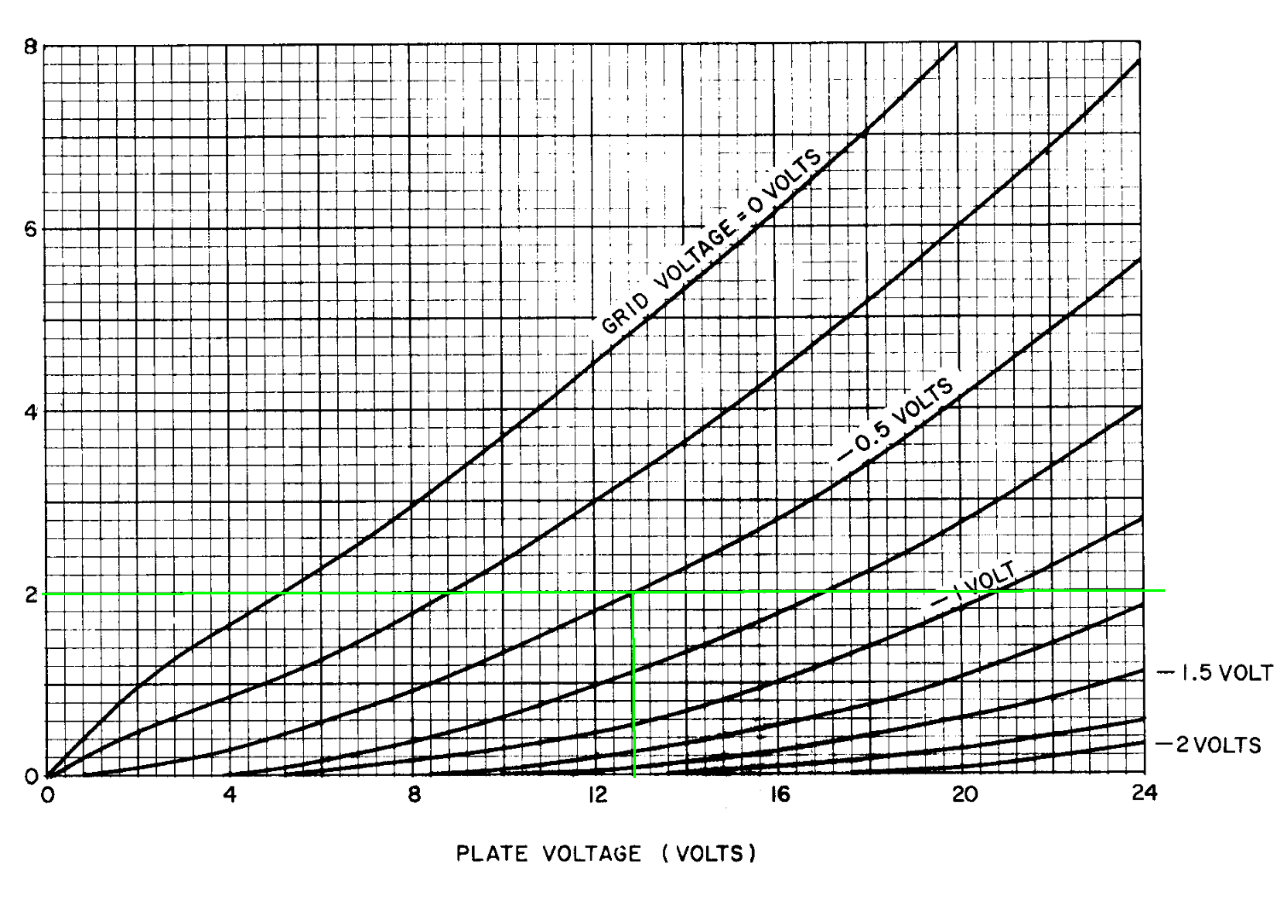
Now, how did I get all these values? First, 20V for the power supply sounded like a decent starting point. That is enough get a few volts swing needed for high impedance headphones, and not out of range for the tube and likely to be fine for the current buffer. Next I drew a load line:
This is very much vibes based, and just a starting point. But this gives 20V/4mA = around 5K for the anode resistor. And 0.5V/1.9mA = around 260 ohms for the cathode resistor. This works, at least, in simulation, and gives about 6 times voltage gain. LTSpice can also calculate the distortion, and that’s around 2.3%… Not exactly hifi! I am not opposed to some distortion, it’s a tube amp with some tube sound, but I’d like to keep it around 1% or so at a good bit of power. After some tinkering around, I didn’t get it much lower, so time to call in some transistory support!
The almighty constant current source
The load line is always diagonal, but often tubes perform better with a more horizontal load line. The higher the anode resistor, the more horizontal the load line (and the higher the voltage gain), but what if we can make it horizontal? For this we would need infinite resistance, but somehow still have current flowing.
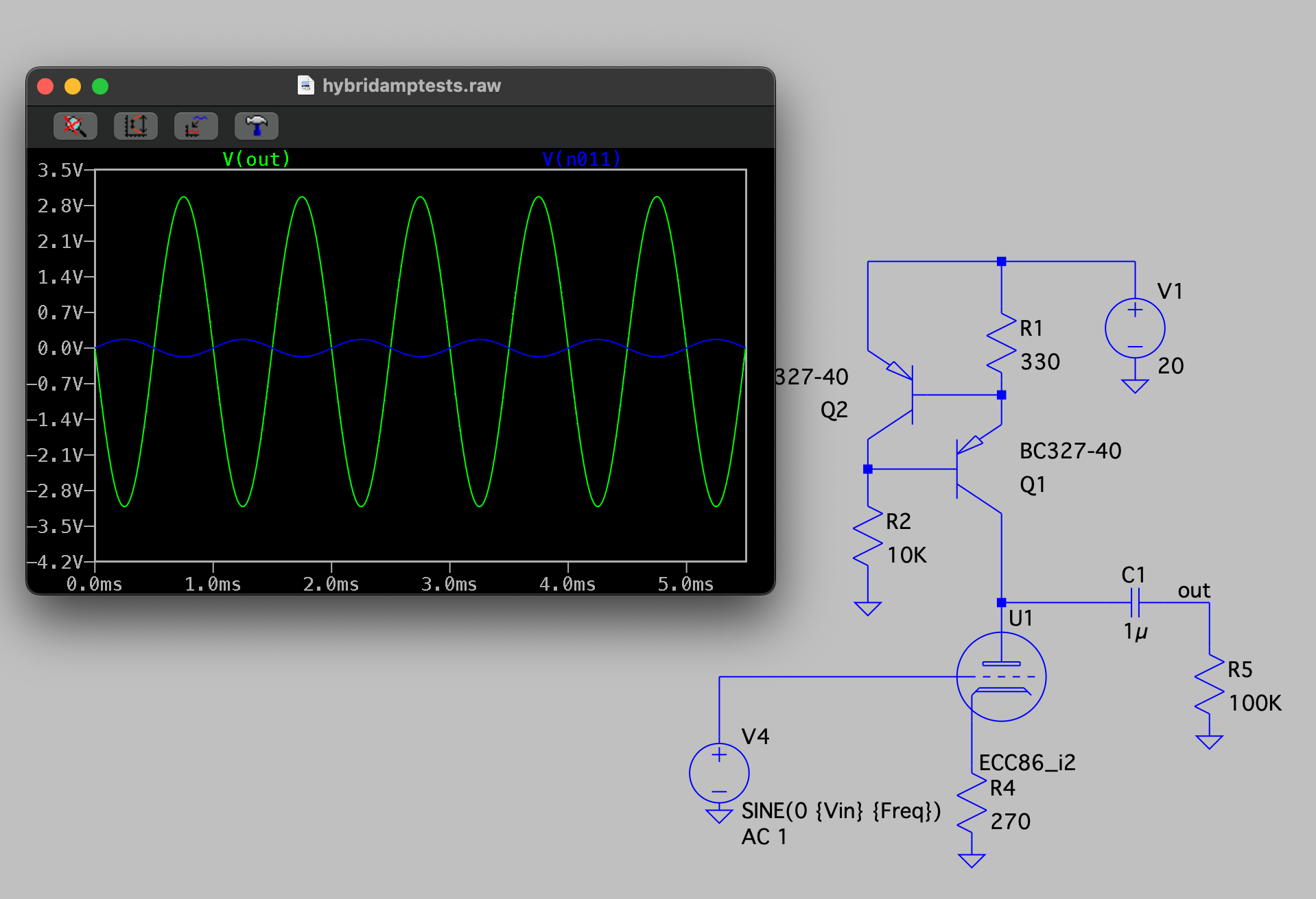
And we can, with a constant current source! Well not perfectly horizontal but a lot better. A simple implementation is the two transistor current source. And because this tube runs on a nice low 20V, cheap low voltage transistors can be used. With this, the load line becomes more like this:
And for the resistors, the current source resistor becomes 0.65V/2mA= around 330 ohms and the cathode resistor stays at around 270 ohms.
First of all, the gain is a lot higher now. To get 3Vpp out, just 0.2Vpp goes in compared to 0.5V for the previous test, so the amplification factor went from 6 to 15 times! Second, the distortion dropped to 1.3%, a big improvement!
I decided to tweak this a bit more, mostly by testing different load lines, and I ended on a 1mA constant current source with again a -0.5V grid voltage. This, in simulation, gives a distortion of around 1%, nice!
There are even more tweaks possible, like a current sink instead of the cathode resistor, but I think this is good enough to continue to the output buffer.
Current gains
As said before, tubes are generally not the best at delivering current, and in order to drive headphones a bit of current is required. Of course, most tube amps use output transformers, but in order to drive almost any headphone, and save a bit on cost, a hybrid approach with some transistors is my idea. I did mention the diamond buffer at the start, so let’s peek into that.
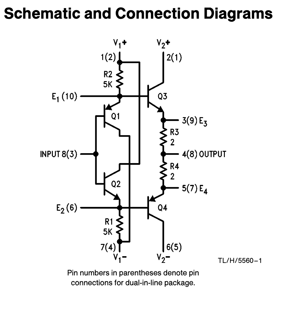
The diamond buffer is a simple, 4 transistor buffer with no voltage gain. Buffers like this used to be sold as an integrated circuit, for example the LH0002. And hey, that datasheet has a schematic, including all values needed. Neat!
4 transistors and 4 resistors is all you need. A quick look at these transistors, R3 and R4 are emitter resistors and help counter the effect of thermal runaway and improve stability of an amplifier.
R1 and R2 set the idle current of the amplifier stage, the lower their value, the higher the idle current through Q1/Q2, which in term affects the idle current through Q3/Q4.
Putting in the values from the LH0002 gives some pretty good results
The output voltage is a tad lower then the output of the tube, but now the load is 32 ohms, a common headphone impedance. And the distortion is still at around 1%
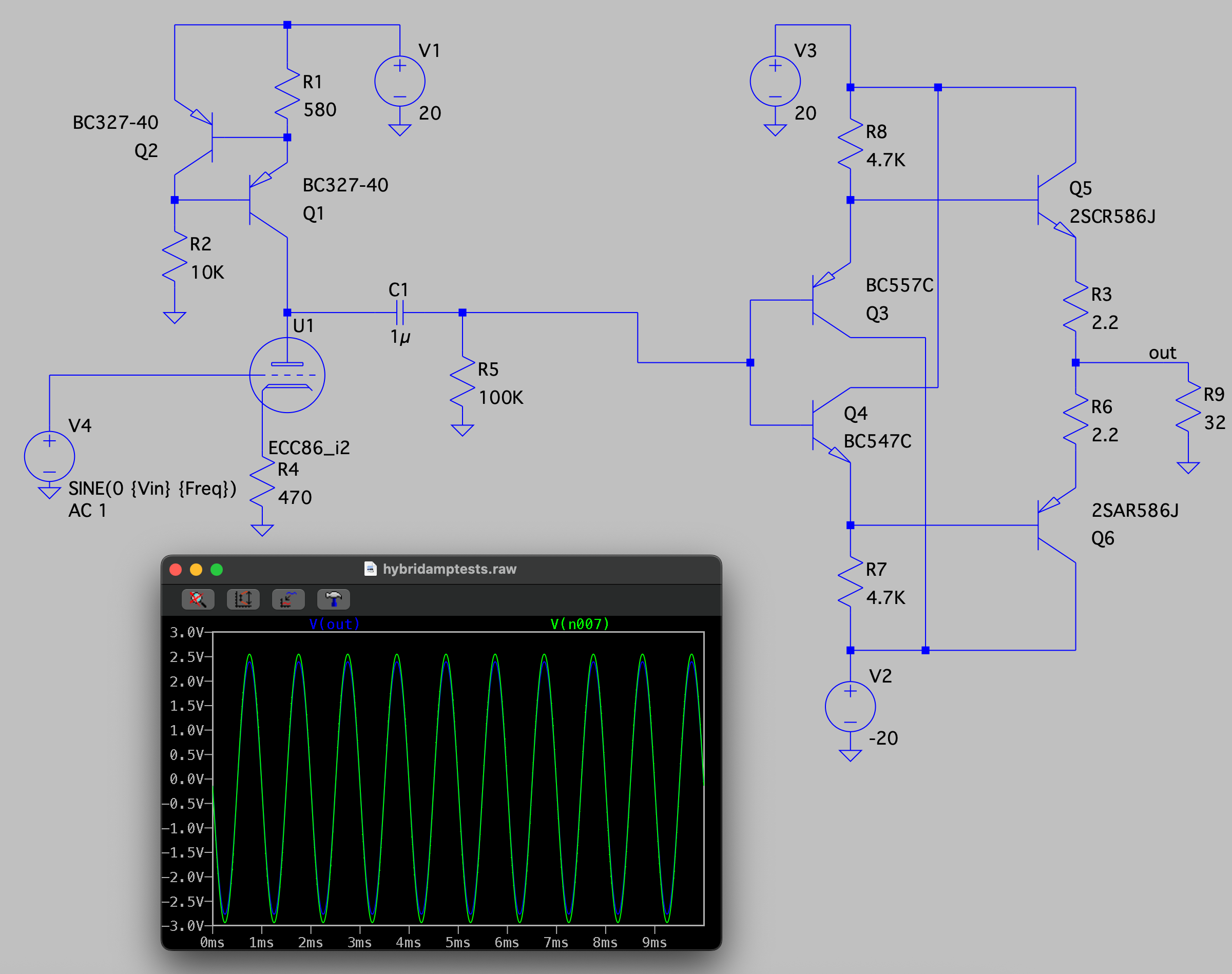
One thing to note is that it’s not perfectly balanced. The output voltage is a little more negative then positive. Making the lower resistor R7 a bit higher in value can fix this issue. There are probably better ways to do so but I do like a simple solution. In the end the schematic I ended up with is the following:
The distortion is around 1% at a good amount of output power. It can drive most headphones and can even deliver a watt into an 8 ohm speaker. So let’s design a PSU and give it a test
The power issue
The 20V I picked seems to be a good voltage, so I’ll stick with that for now. This means +20V, -20V and of course 6.3V for the ECC86 filament. One thing to keep in mind is that with a triode amplifier like this, the power supply must be pretty clean of hum and noise.
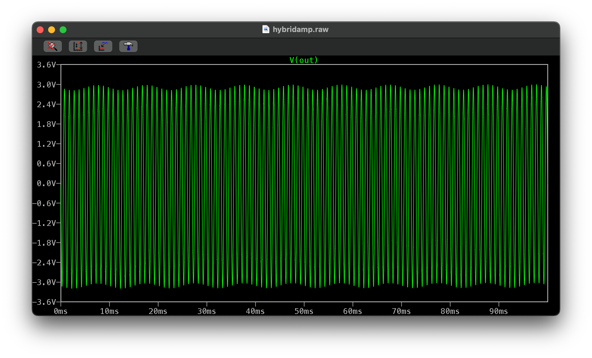
If there is 2V of 100Hz noise on the 20V line, this is clearly visible (and audible!) in the output. A quick check shows that there is roughly 170mVpp in the output left, so the so called power supply rejection ratio of this stage is pretty poor.
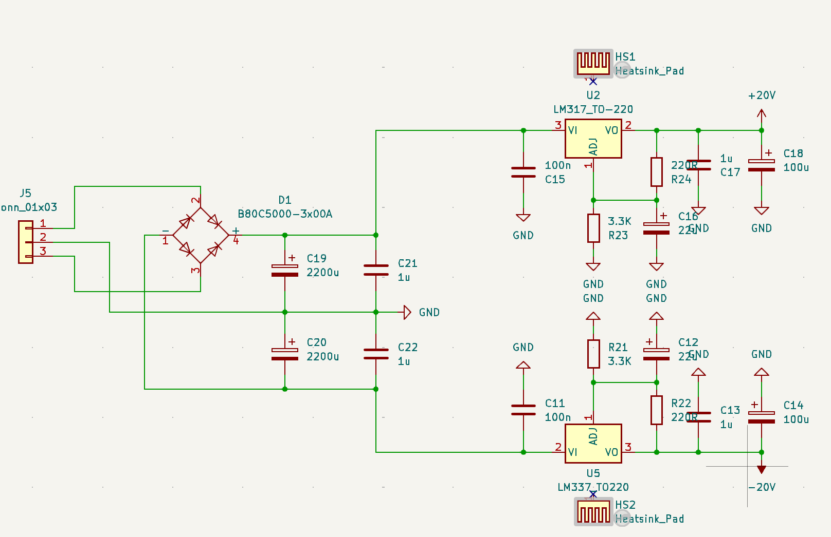
So to improve this, I added linear regulators for each voltage rail. The less noise in, the less noise on the output!
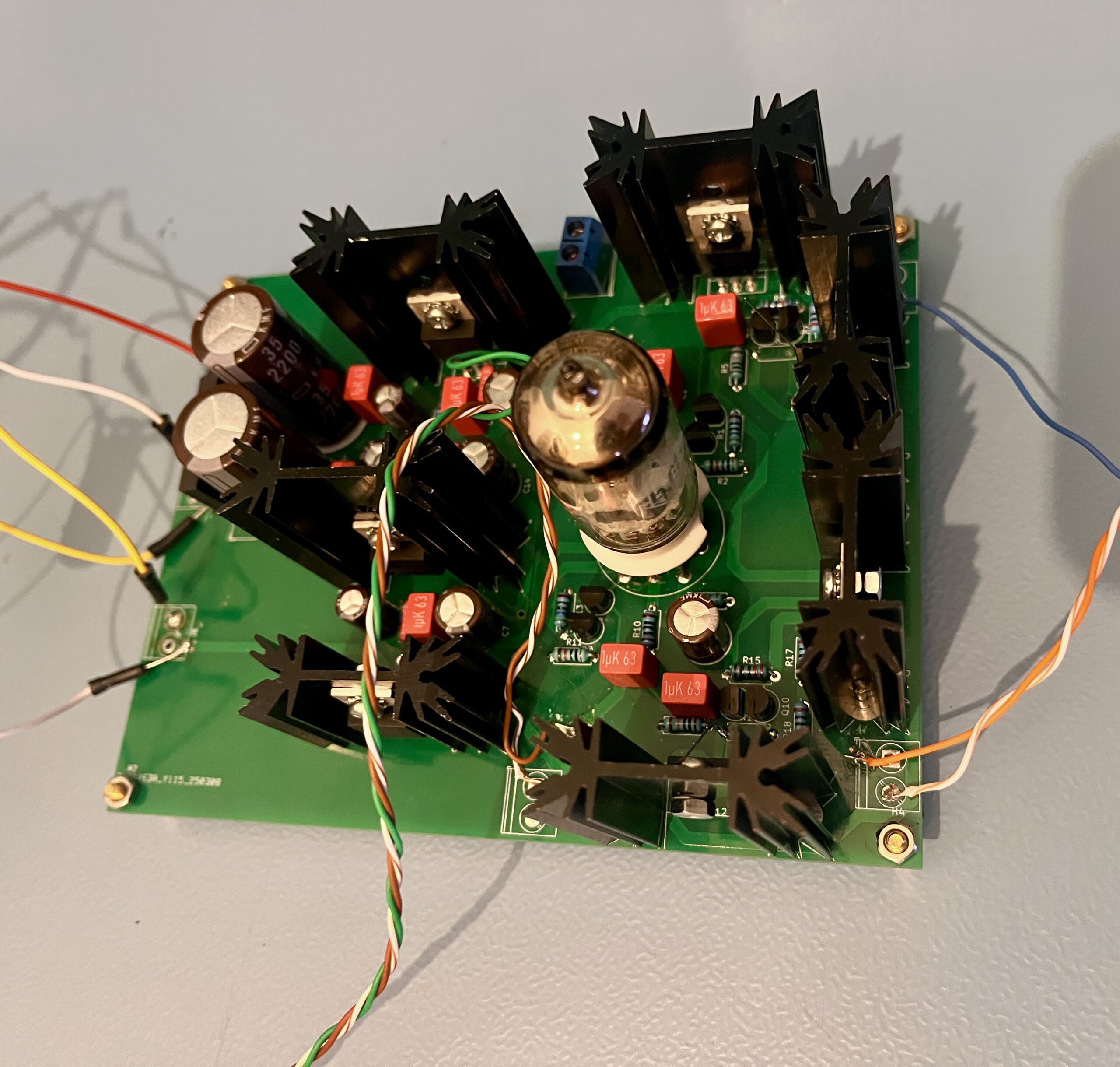
Nothing too spectacular, just the good old LM317/337 with some heatsinks. A bit of routing later I ordered some PCBs and parts to build.
Theory to reality
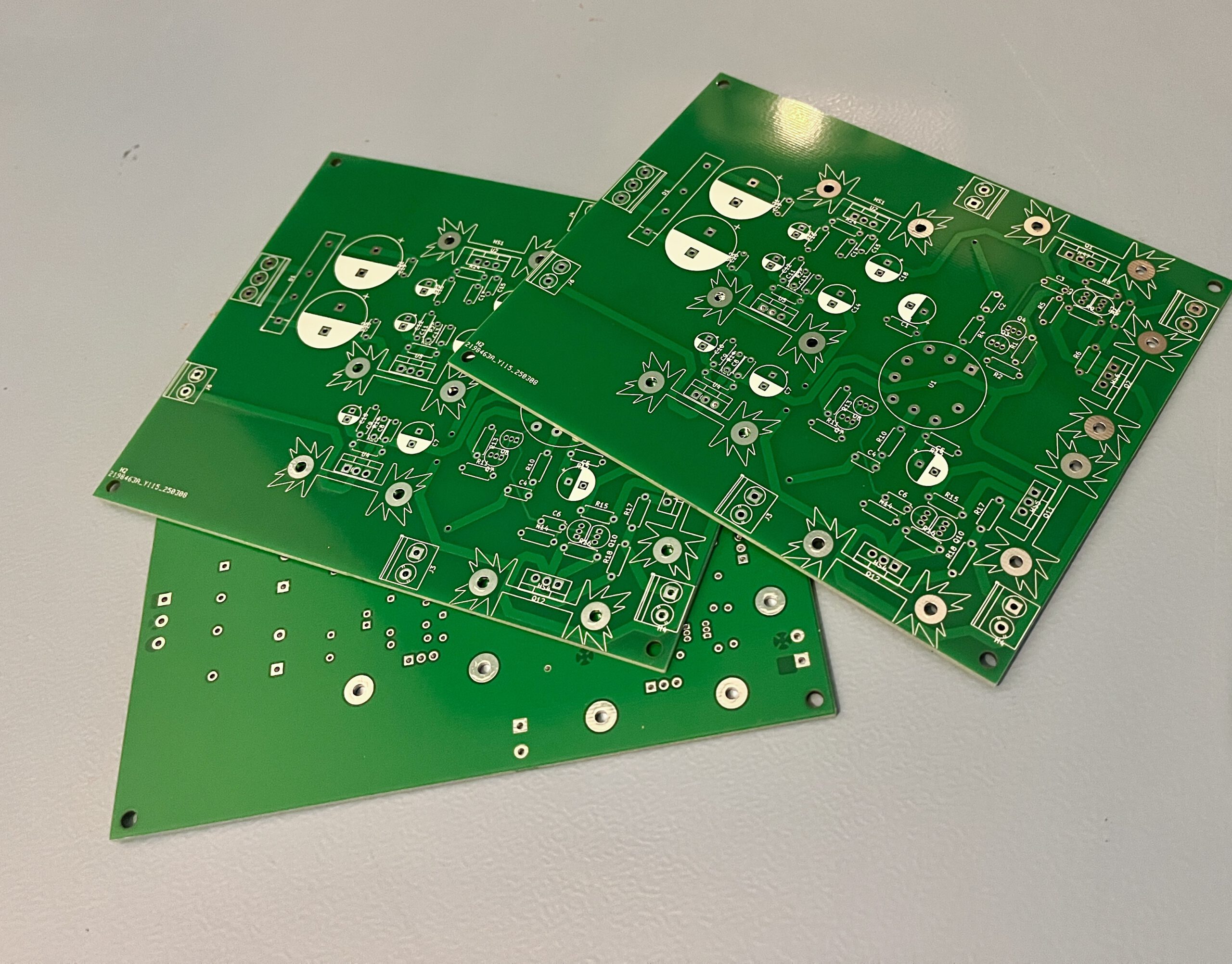
So with some PCBs in, I noticed one very stupid mistake. I moved a few connectors, but I did not update the copper pours… This means there are some shorts to ground on the PCB. Luckily fixable by cutting through a few traces and patching it. When soldering I also spotted a few more small issues. The footprint for the tube socket was incorrect and the LM337 was 180 degrees rotated so I could not mount it to the heatsink. All very fixable but very much “I rushed this a bit” PCB layout mistakes :) But in the end, the result is this:
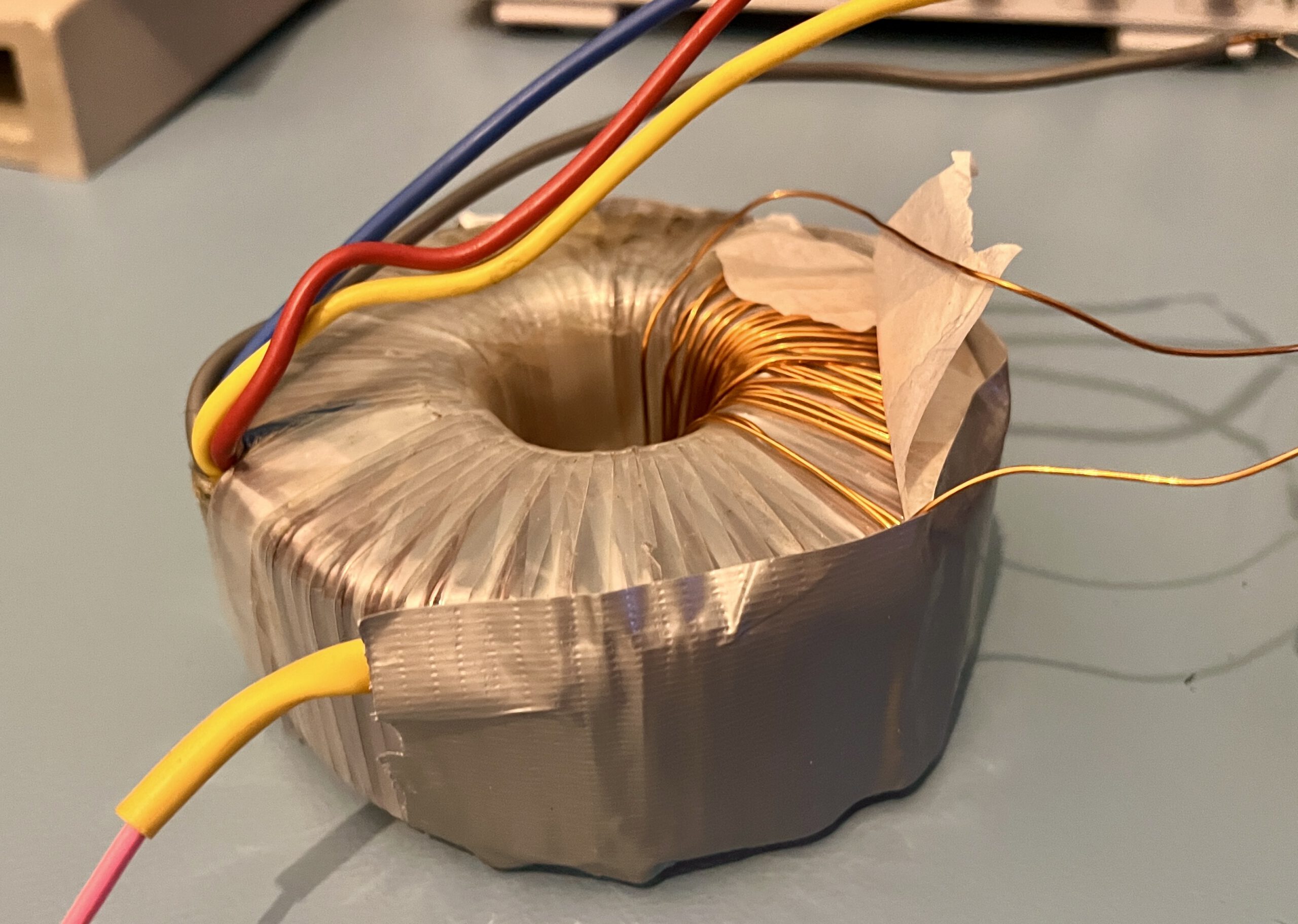
Now, one thing to note is the transformer. Finding one with 2*18V or so, and an extra tap for the filament is quite difficult. Luckily with a toroidal transformer, you can just add a new winding. A great guide on this can be found here. With some good enough transformer I had laying around, I ended up adding about 30 windings for 8VAC. Perfect!
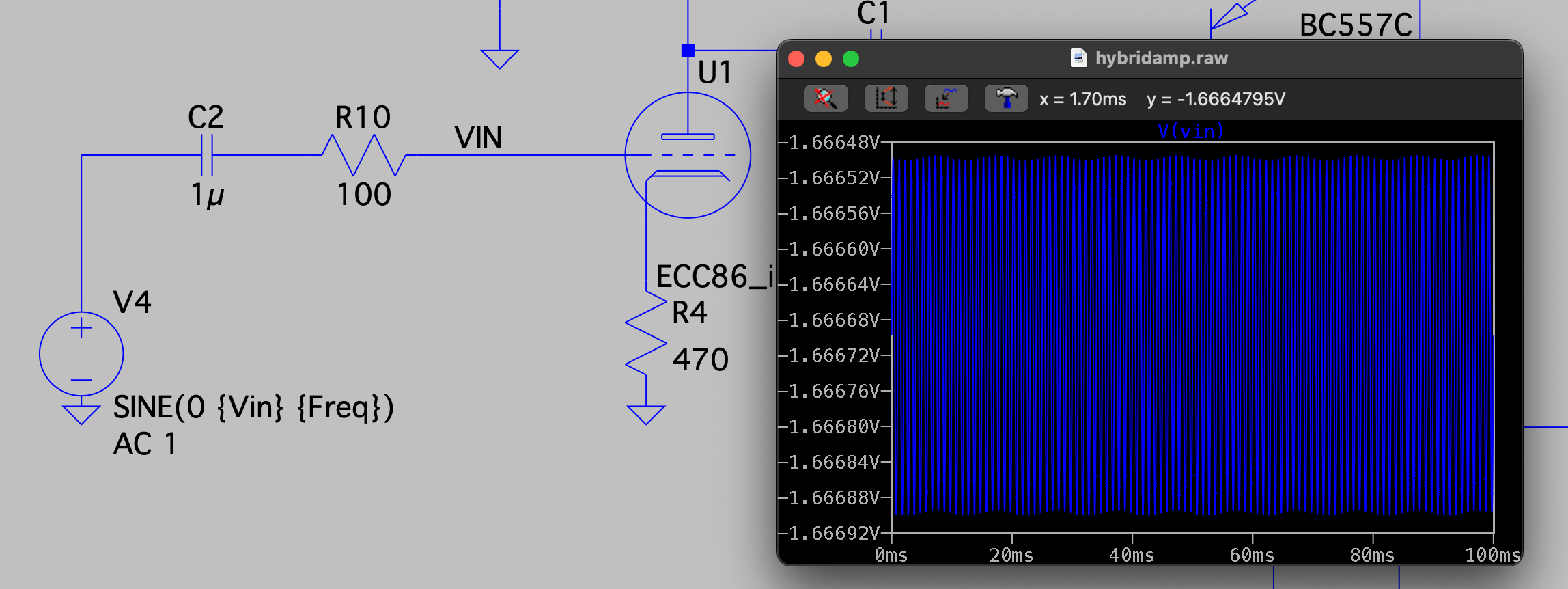
But, does it work? Well. Another few mistakes where found, one was that the voltage on the grid of the ECC86 was a few hundred mullivolts negative! This didn’t show in LTSpice as I added a series capacitor to block DC, but I added them in Kicad and never in LTSpice.
Adding that in LTSpice and indeed, the input is pulled low!
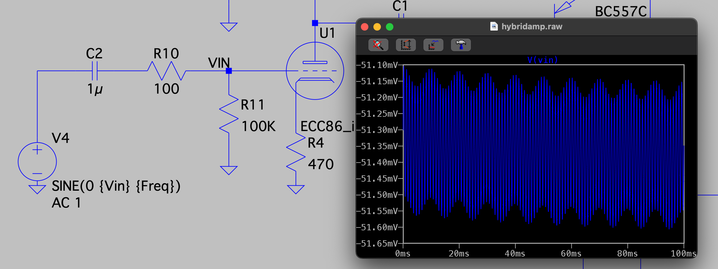
This is because tubes have some DC current on the grid, so a pull-down resistor, called a grid leak resistor, needs to be added. Otherwise the DC current builds up in the capacitor causing the voltage to go quite negative. Adding a 100K resistor helps a ton:
Apart from that, it all worked as expected and all the voltages like the biasing of the tube matched the simulation pretty well! So I call that a success for sure.
What’s next and improvements
With the bunch of small mistakes, I decided to make a new PCB to solve all these. Other issues I want to look at are adding a potmeter for volume, and thermal coupling of the diamond buffers. One thing I didn’t do what have all four transistors thermally coupled, so connected to the same heatsink. For a diamond buffer this is good practice to do to help against the idle current not slowly drifting up and causing thermal runaway.
Of course, this all needs a nice case too, something like the modu galaxy series with a custom front/back would be lovely I’d reckon.
But for now, this blog is long enough, so let’s deal with that a next time! As always, if you enjoyed this blog, you can buy me a coffee!
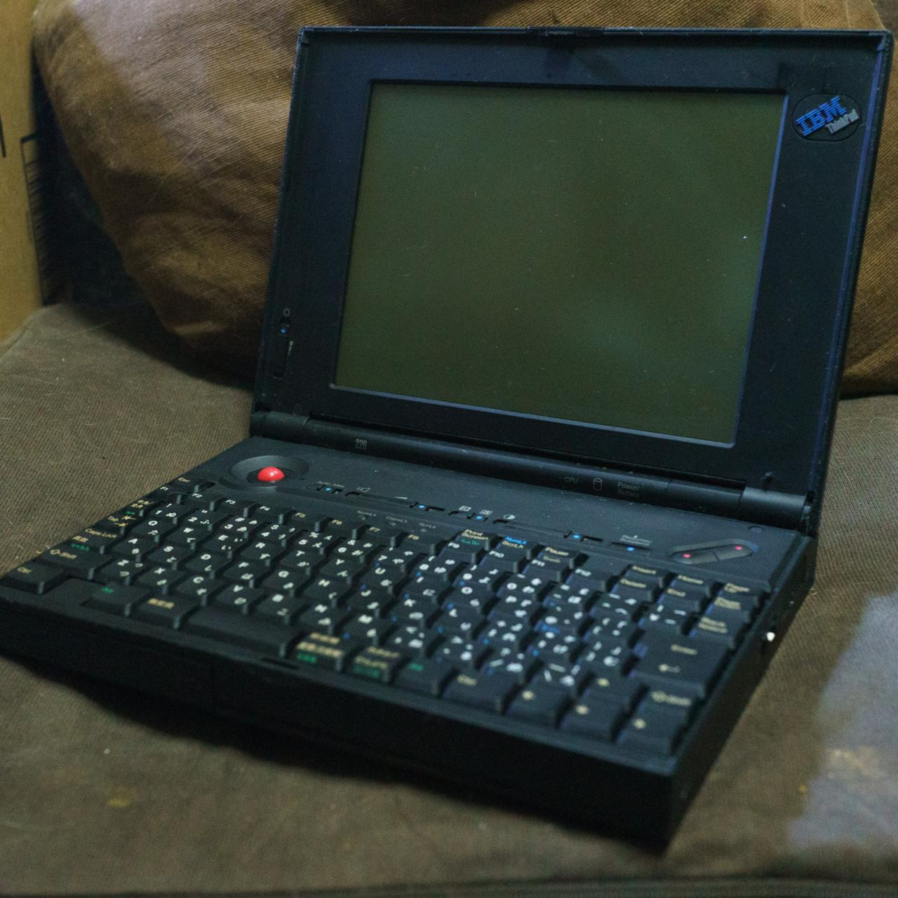
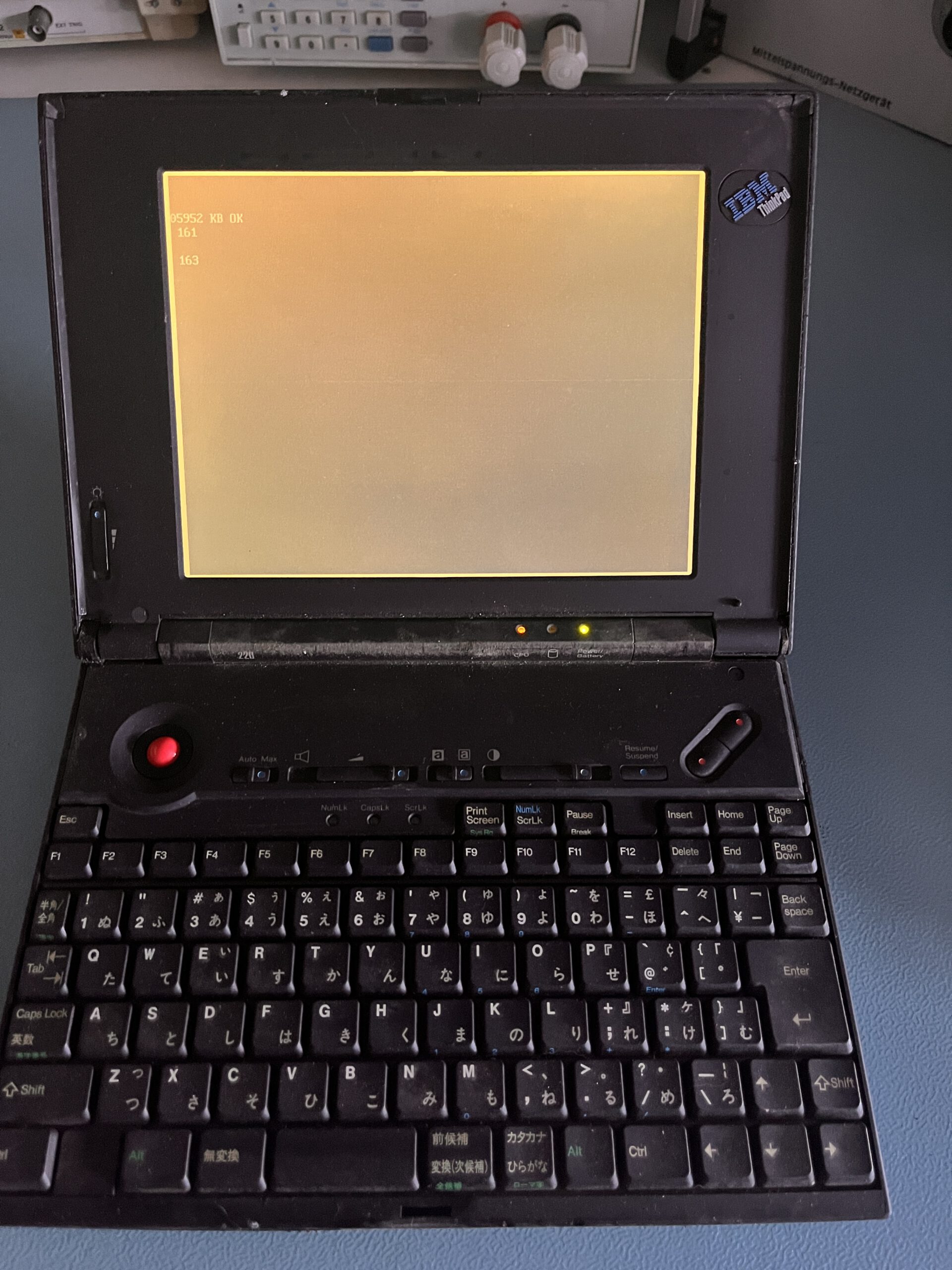
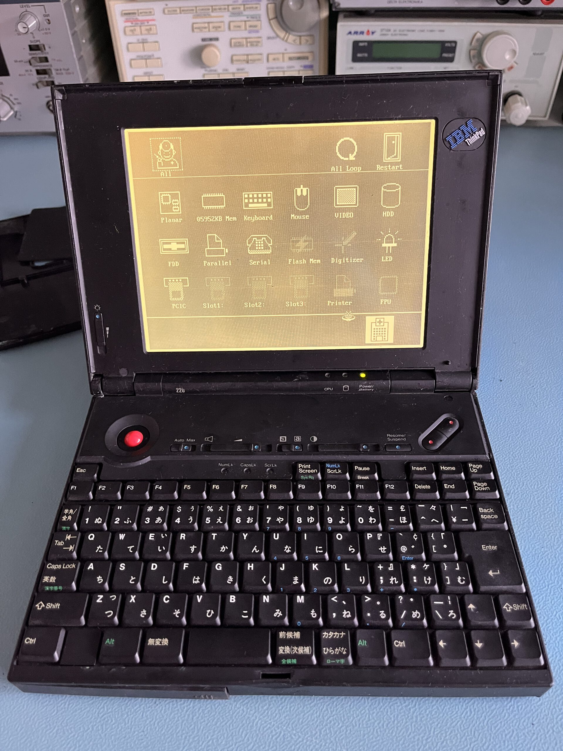
More old tech, more blog posts. This time about a Thinkpad 220. No, not the X220, the 220. A 1993 vintage, Japan only, ultra compact Thinkpad! There is not much online about these so let’s fix that!
I saw one of these laptops for sale, untested, on Marktplaats. A Dutch Ebay so to say. It was looking a little rough but the fact that this laptop popped up at all was amazing, and luckily my offer got accepted. So a few days later I was greeted with a dirty laptop. No adapter or anything, just a laptop.
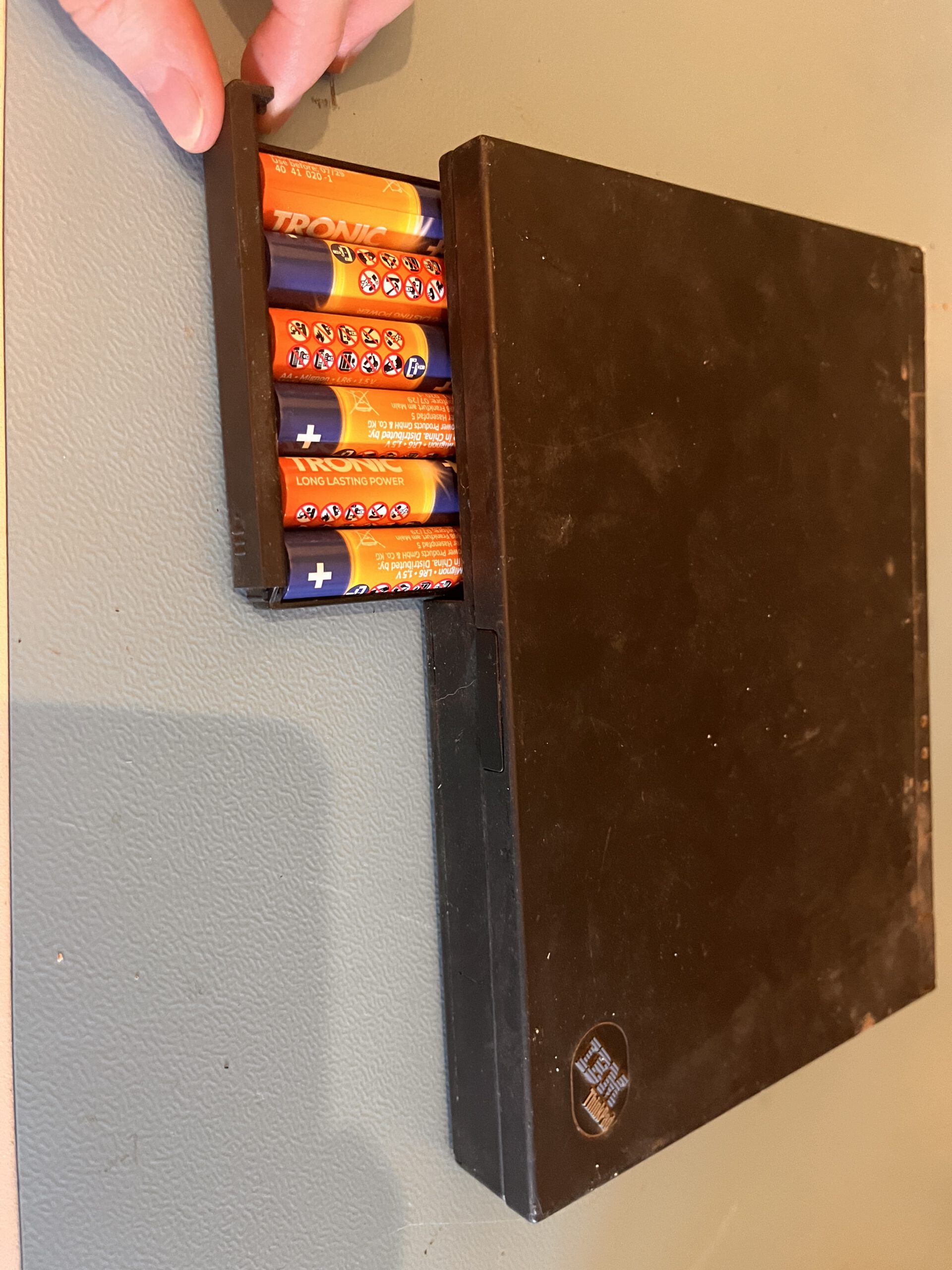
Luckily, powering this laptop is oddly easy. It just takes some AAs
Oh yes. Just stuff some AAs in it. I like it! Now, just alkaline AAs work, sadly there is no support for rechargables.
And it just works. Huh. Well there are a few errors related to an empty cmos battery, which is not surprising at all. So, it just needs a clean! Which means a full disassembly. Which there is zero info about online.
Guess why I am typing this blog :)
First, some history
This Thinkpad was launched in 1993, and it was made by IBM and Ricoh, just like the more known PC 110. That laptop is is even smaller but has a cramped keyboard and made a few years later. Like the PC 110, this was only sold in Japan. They really like their small computers over there!
Specs wise, you’d get an Intel 386, 2 to 6MB RAM and an 80MB HDD. This all in a 1KG package, less then even most modern laptops! The screen is 640*480 monochrome and has some backlight.
The 220 initially was a 10th year anniversary addition for the IBM 5550 and apparently IBM made 5550 of them and they where popular enough they ended up selling 20.000! These where sold for around 200.00 yen in 1993, which is around 230.00 yen today, as the inflation in Japan is quite low. That’s still around 1500 USD today!
A peek underneath
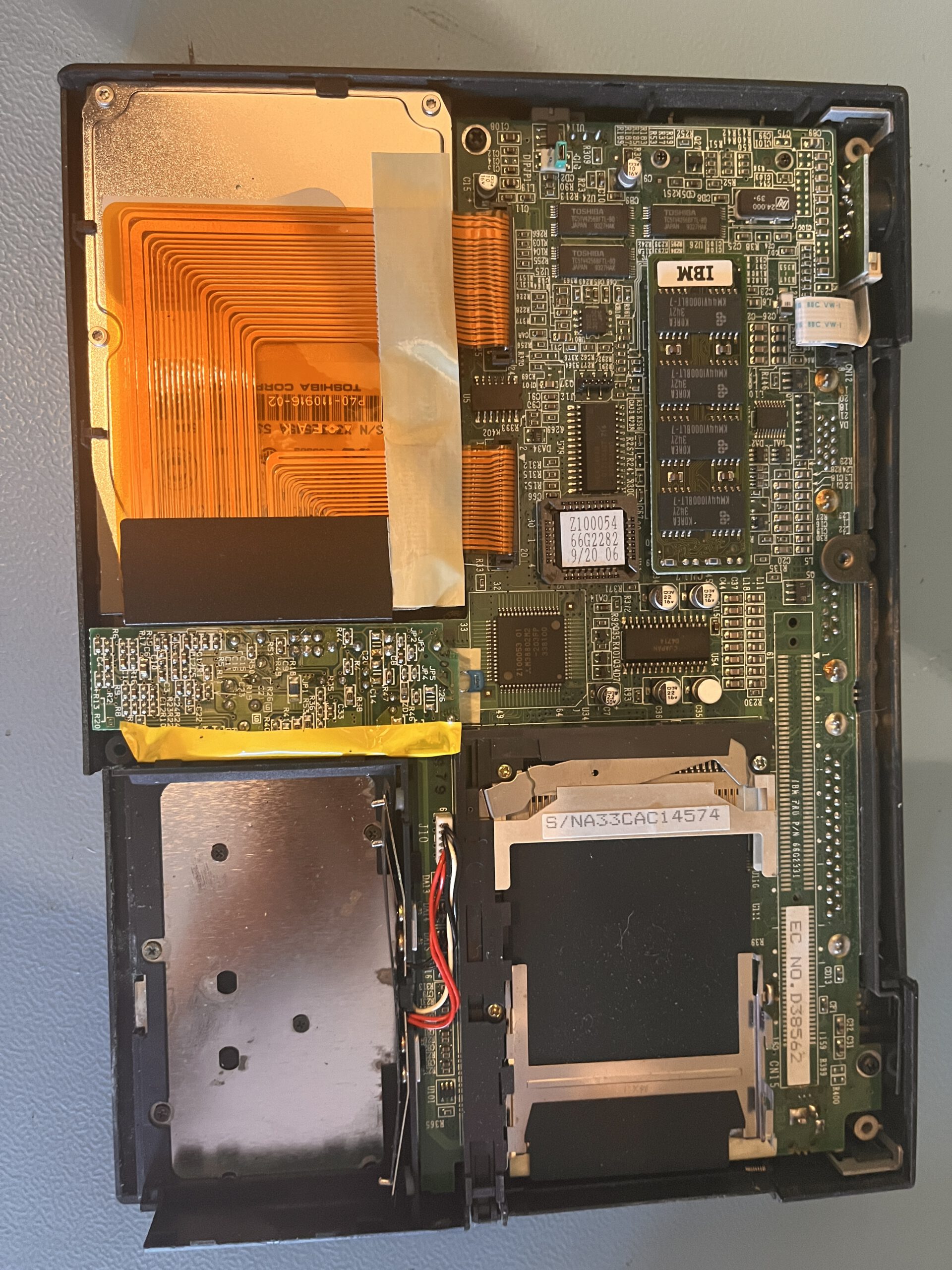
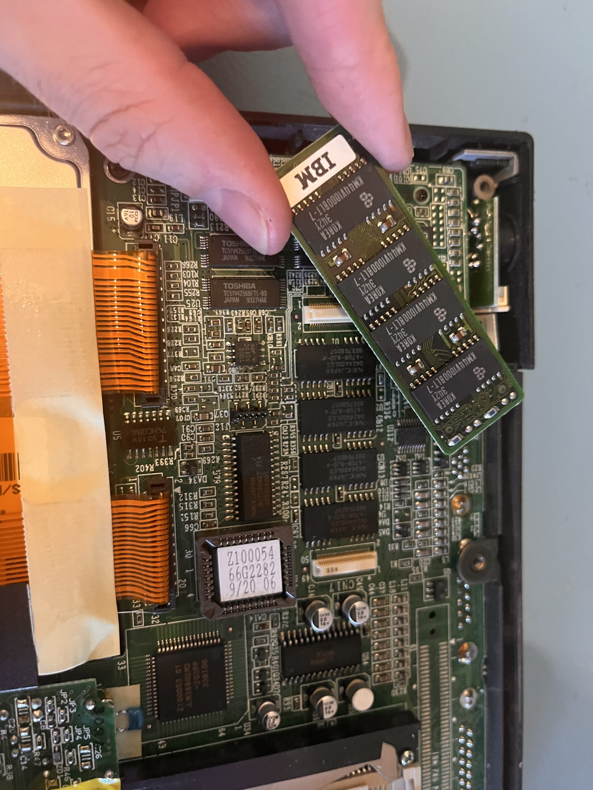
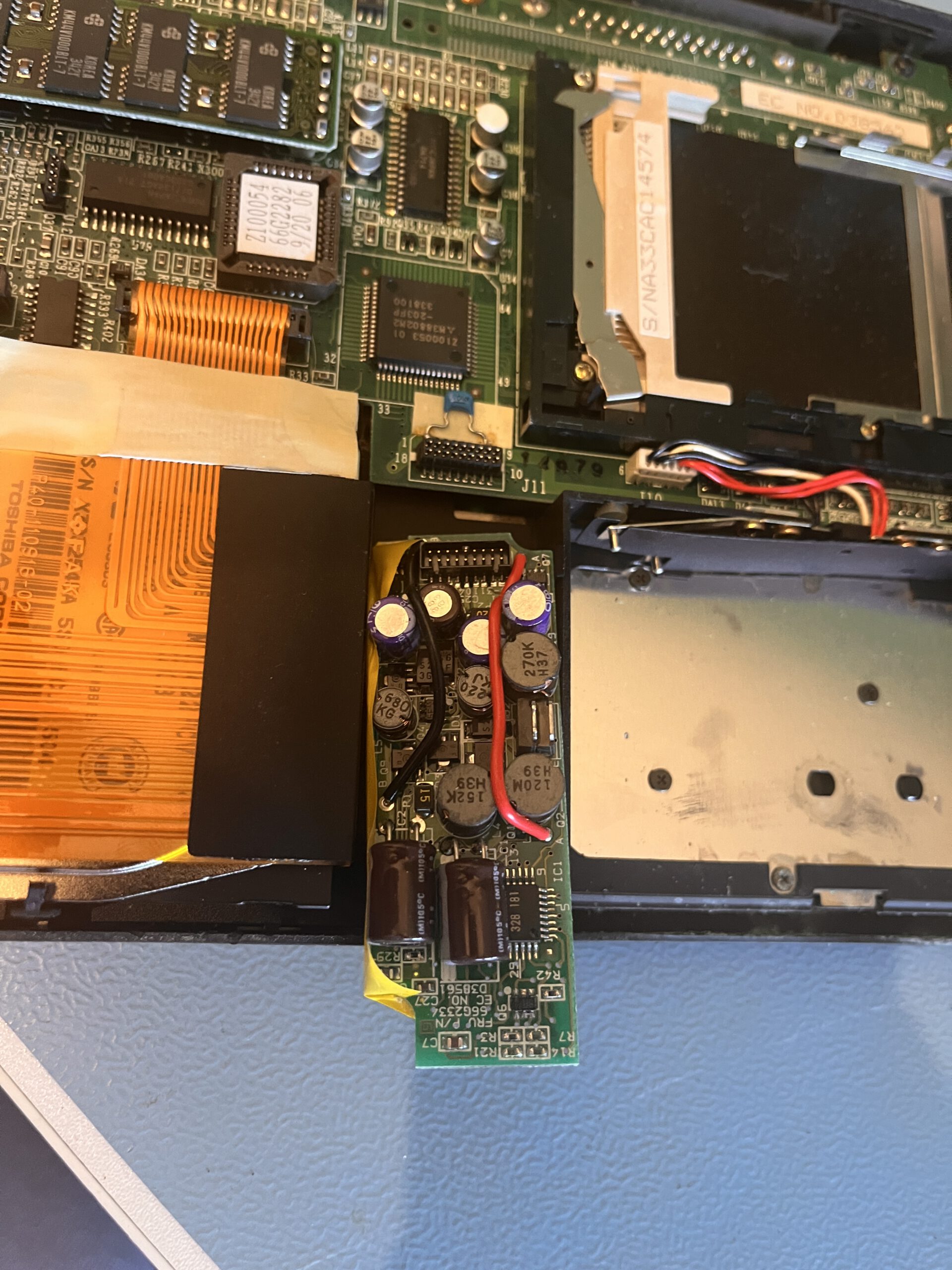
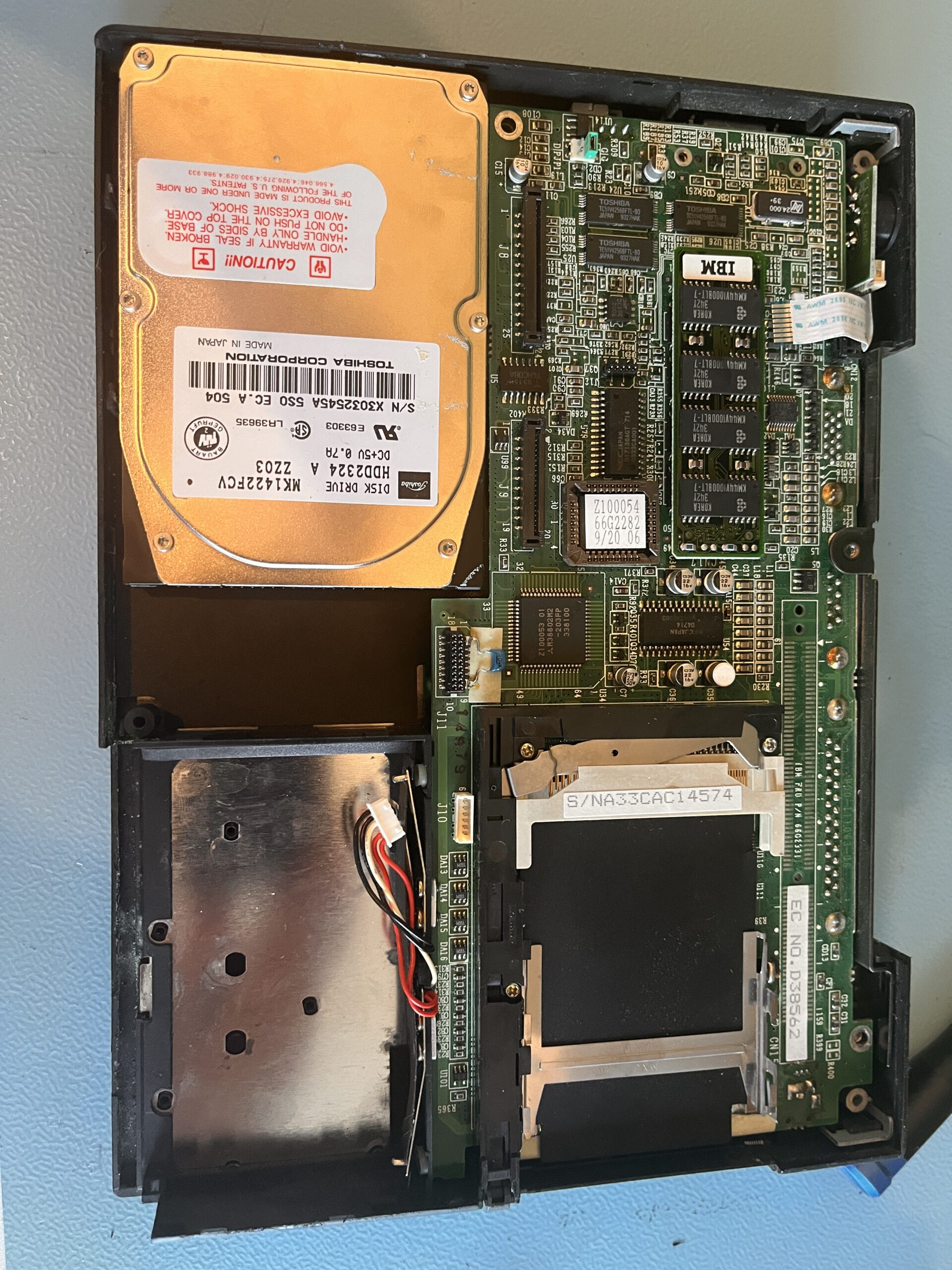
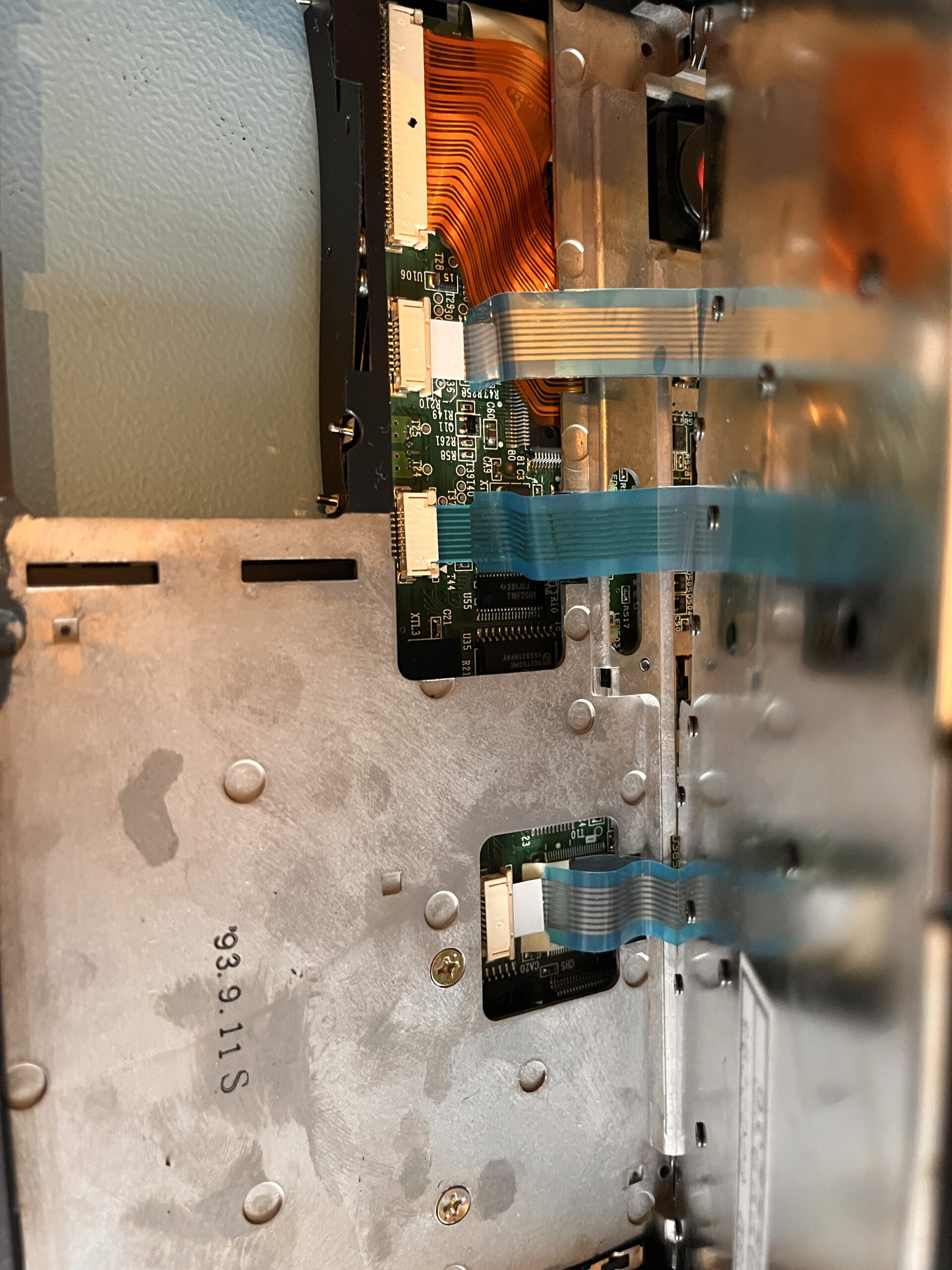
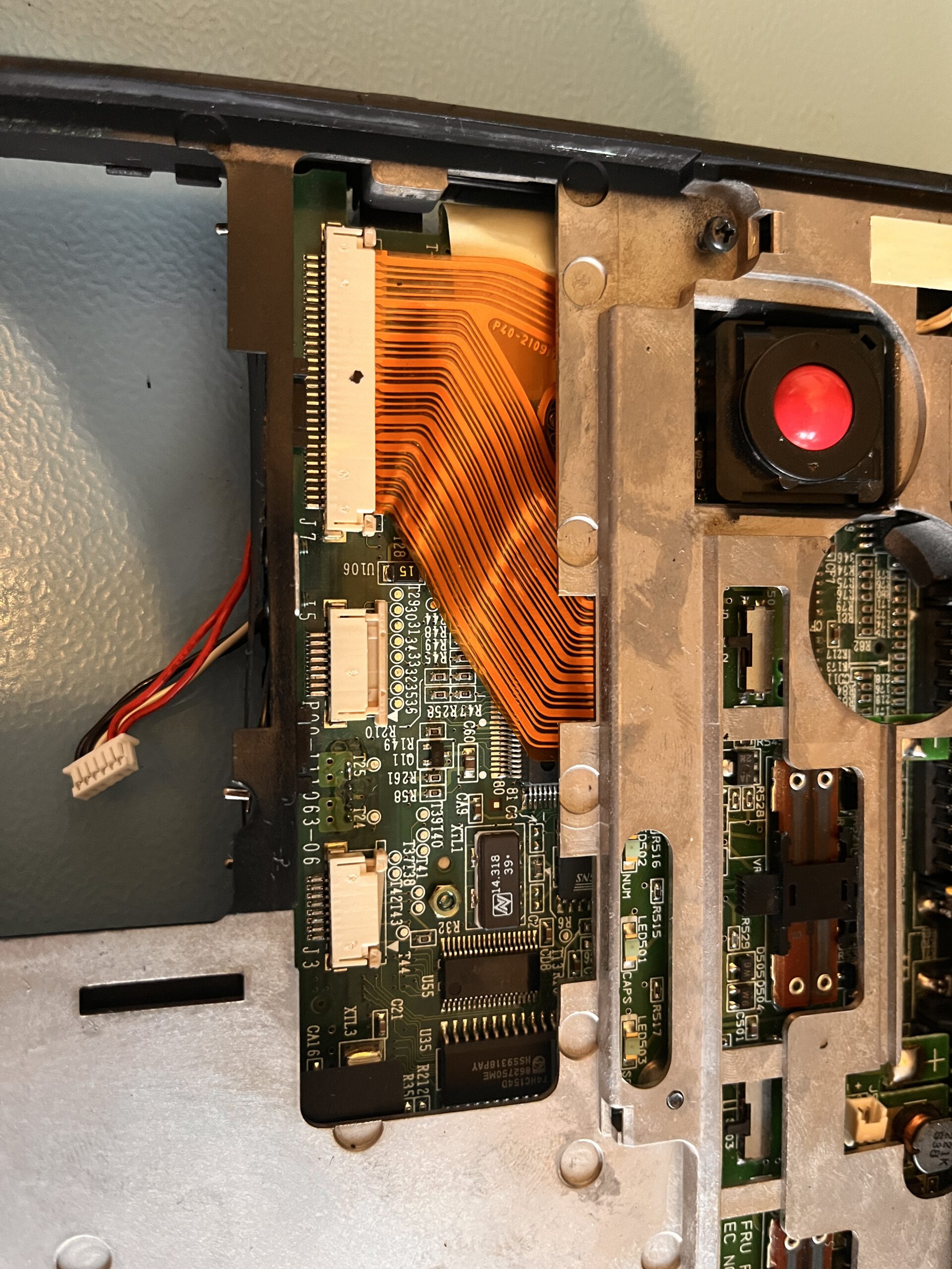
After removing the battery pack, the bottom comes off with a few screws. And there is a few fun things under here. First of all, upgradable memory! There is 2MB on the motherboard, but the optional module can extend it up to 6MB. On my machine it’s maxed out. And there is a power supply module kinda just plugged in there. Let’s remove those two things for now.
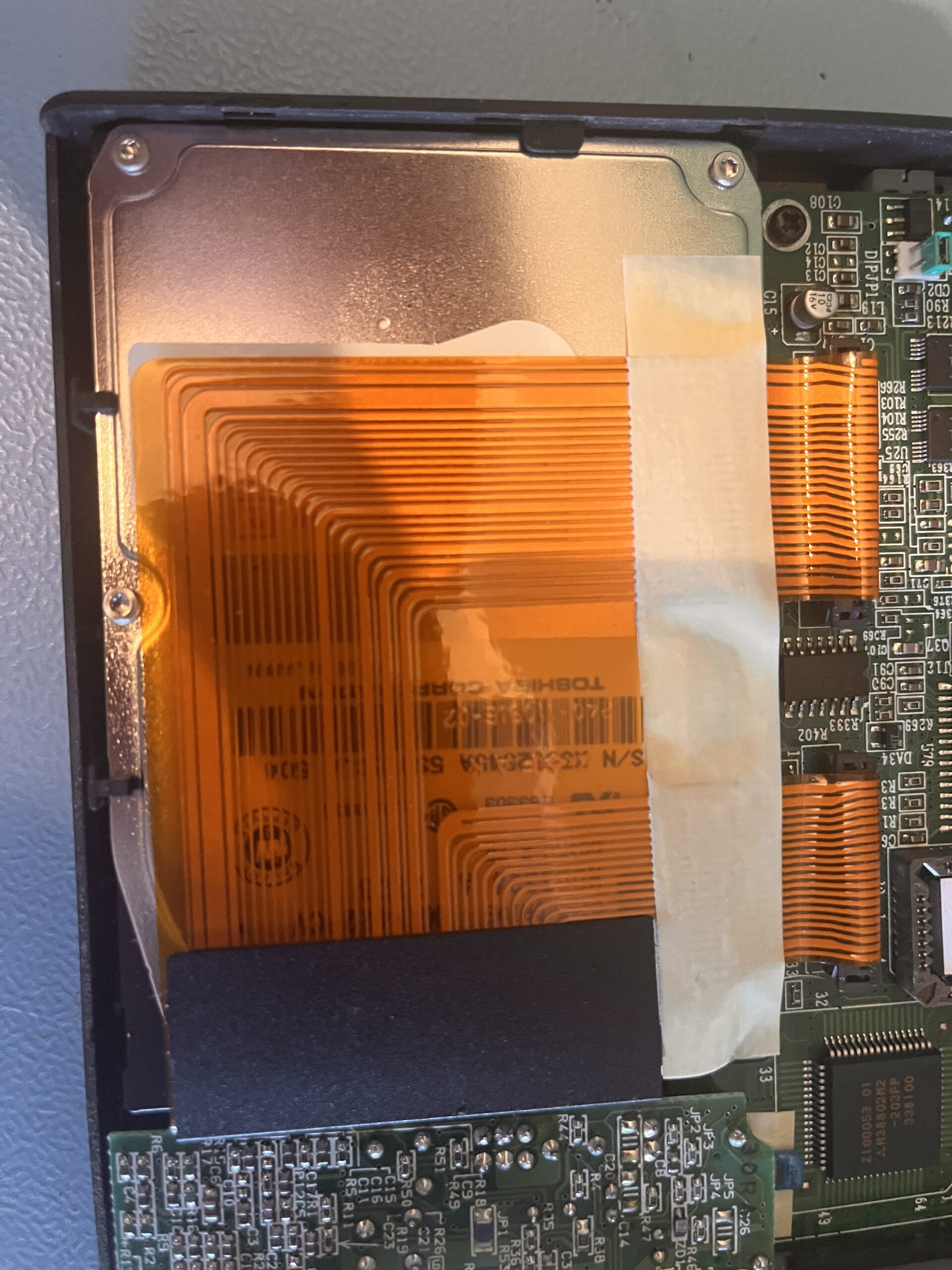
After removing the big ribbon cable, the HDD can be seen but cannot be accessed from the bottom. It’s screwed in from, it appears like, the top. So let’s soldier on and disassemble it more.
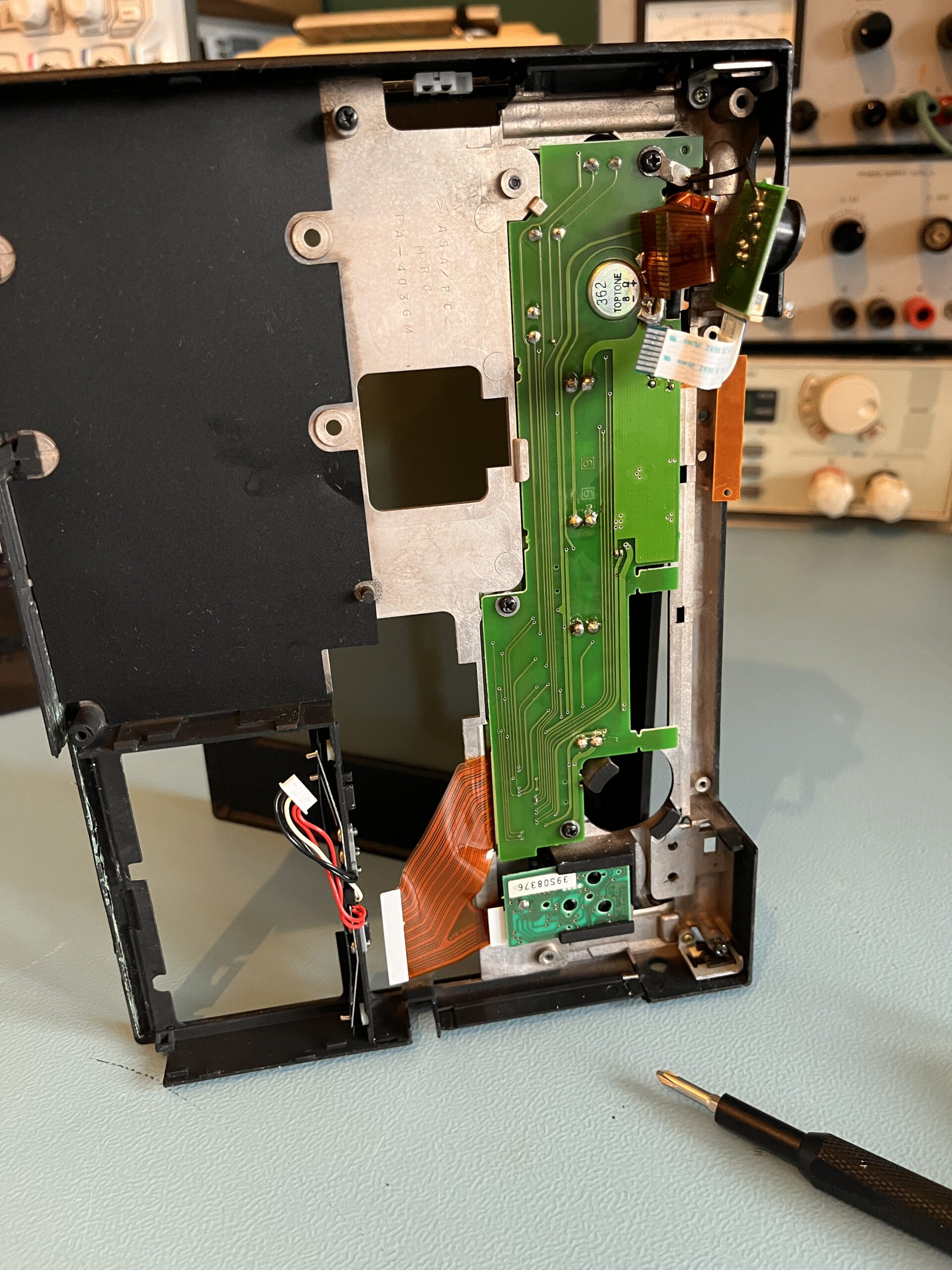
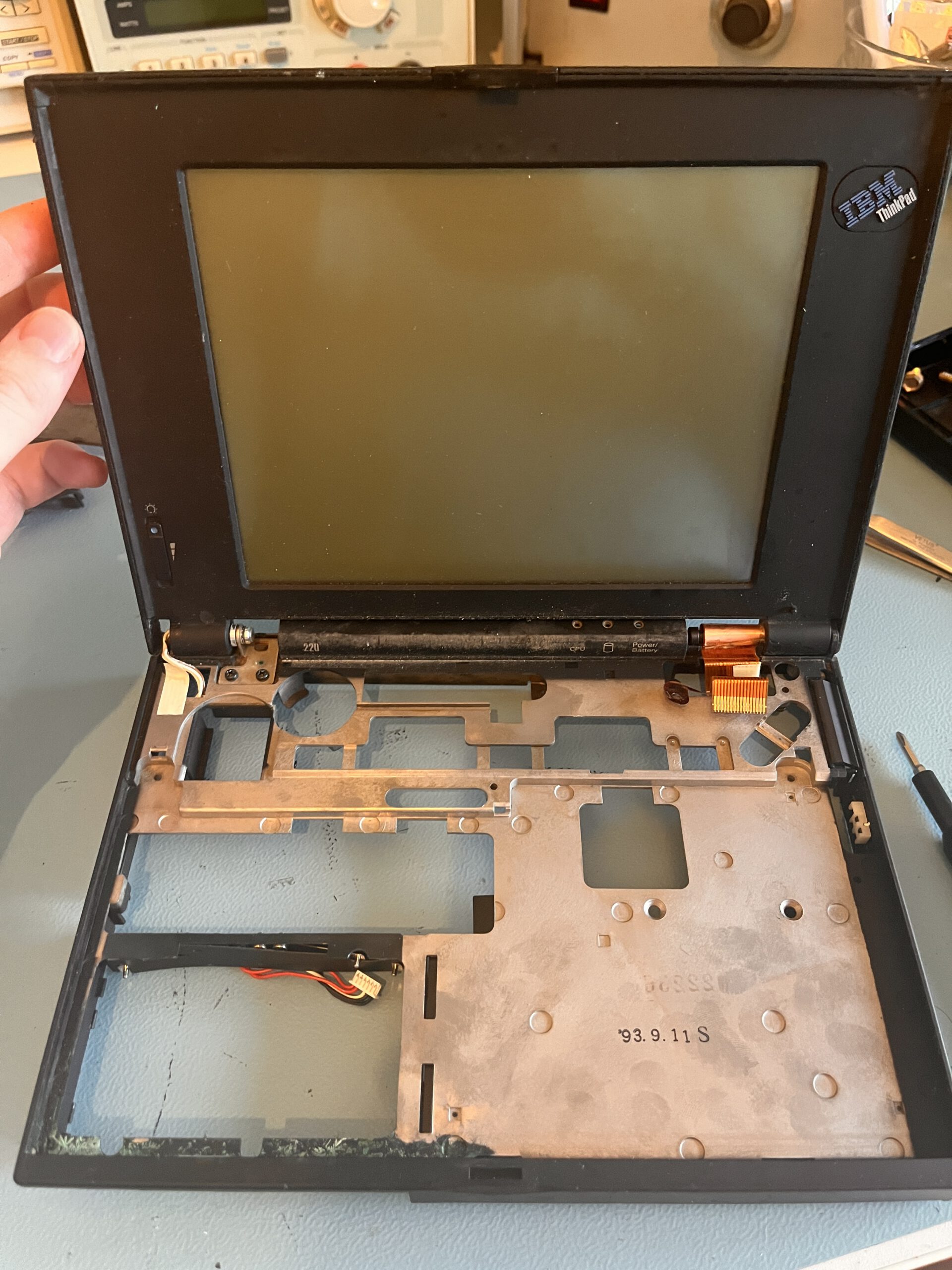
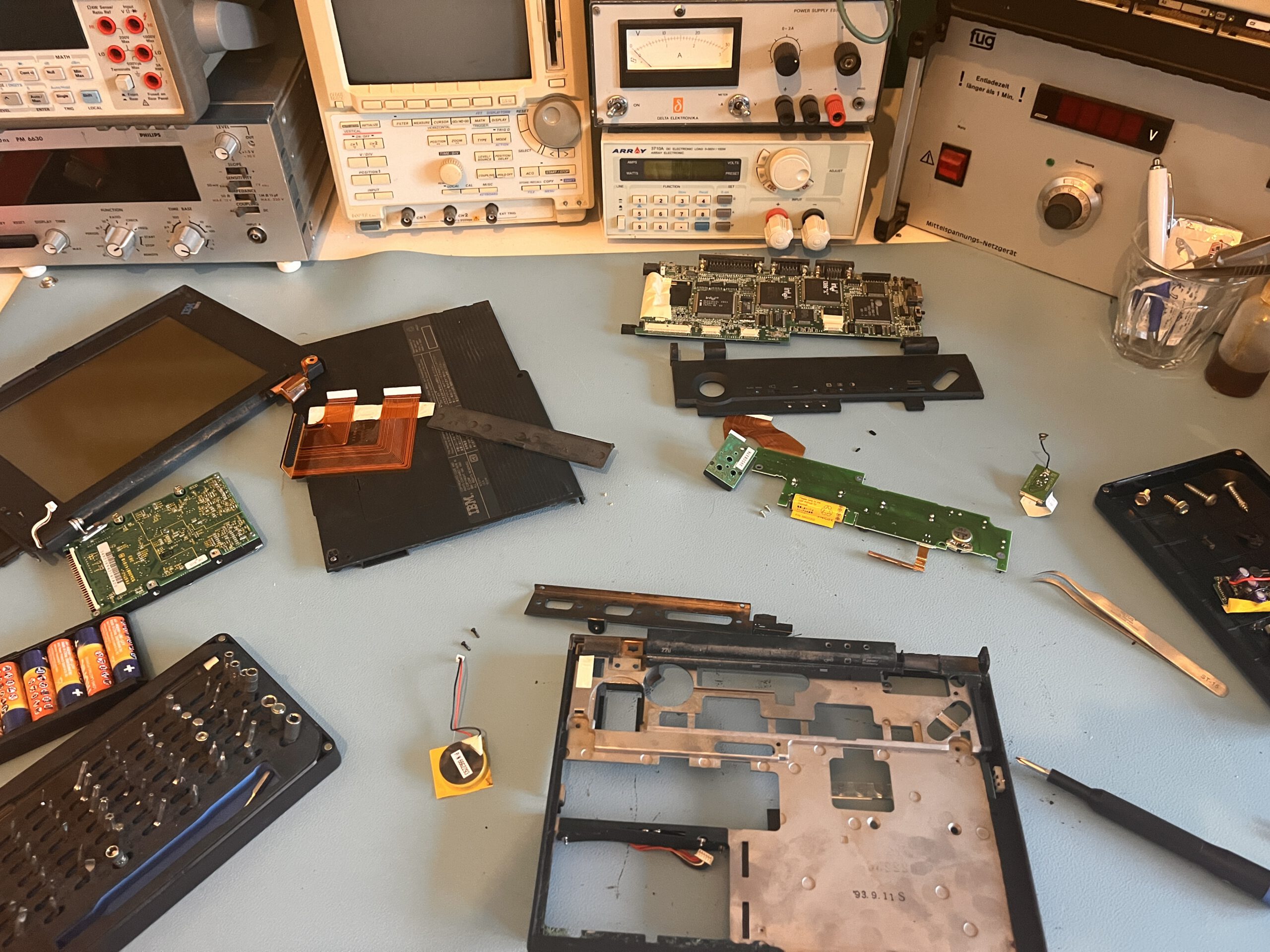
After all screws are removed from the bottom side. the top plastic can carefully be popped off. 2 more screws and the keyboard can be removed. And after all this, finally, the HDD can be removed! Now, for a full disassemble, a few more parts need to come out.
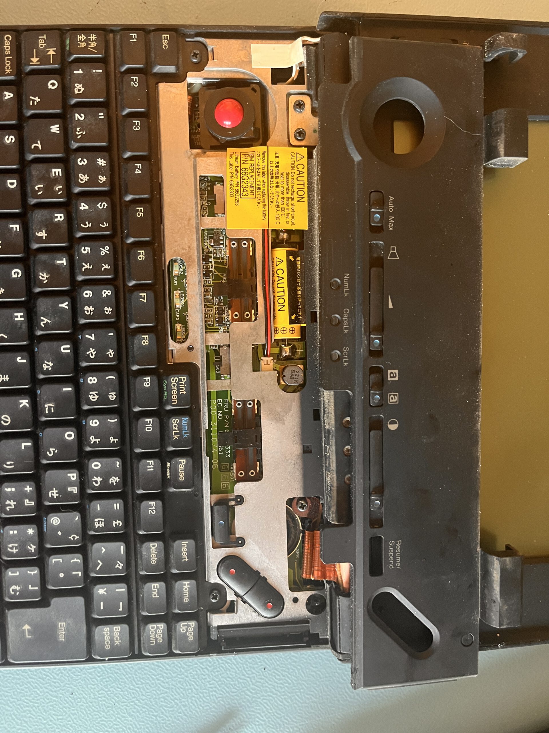
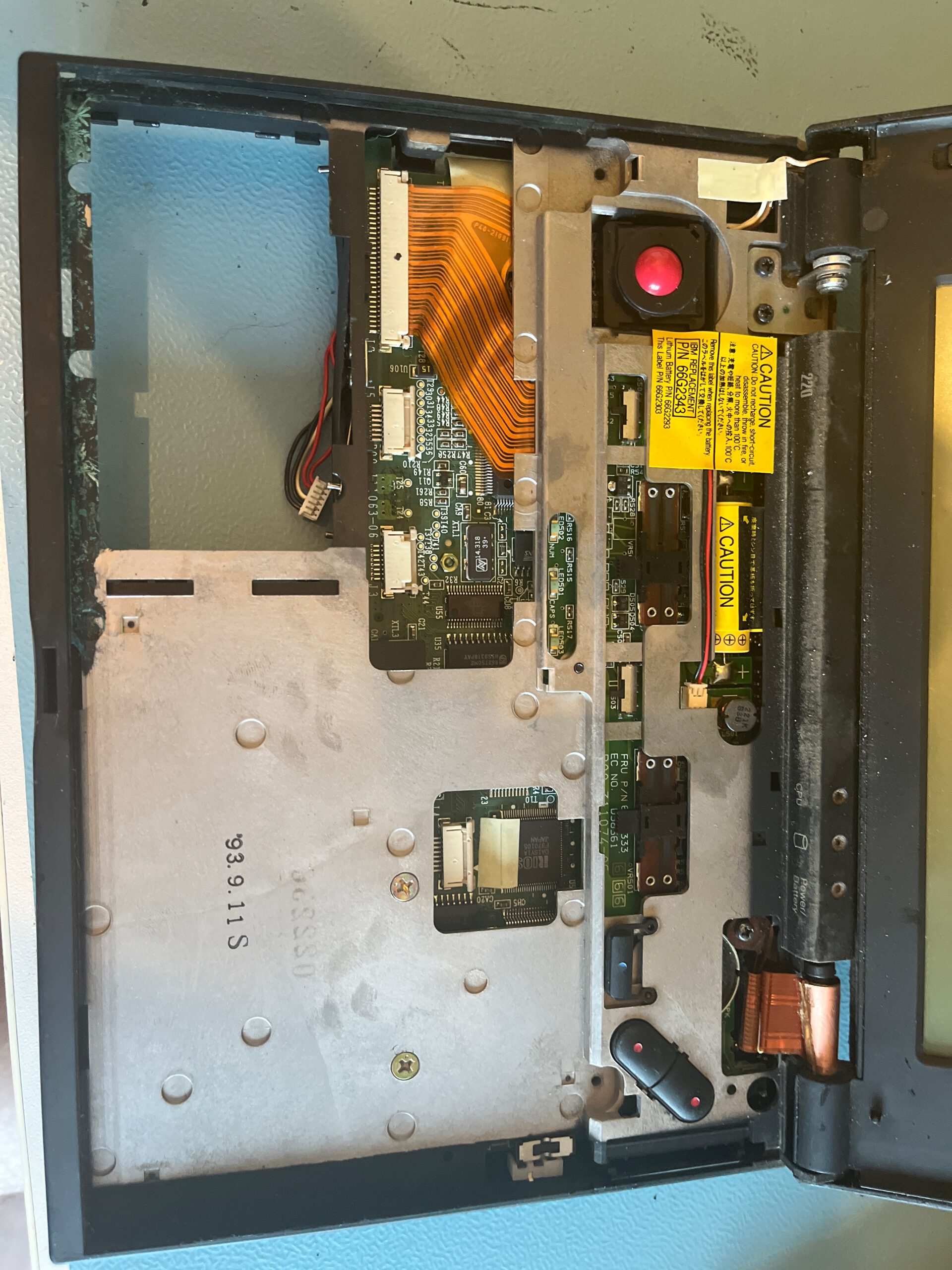
And there we go. There is a small PCB on the bottom for all the miscellaneous parts, trackball, speaker, leds and all that. This also contains a small rechargeable li-ion, which is very dead by now. It’s used for suspend to ram but the machine works fine without. I decided to remove it before it can leak. A small gotcha is in the floppy connector, it has 2 screws. I missed those at first and could not get the motherboard out!
Time for a clean
With everything apart, cleaning this machine is pretty easy! I tend to clean mostly with a degreaser, warm water and patience. The plastic on older Thinkpads can get sticky sometimes, but this one seems fine so far luckily!
After that, it’s just reassembling, carefully, and there we go, a nice and clean machine!
Perhaps this will help someone in the future, as these laptops seem quite rare and hard to find info about. And as always, welcome yo buy me a coffee!
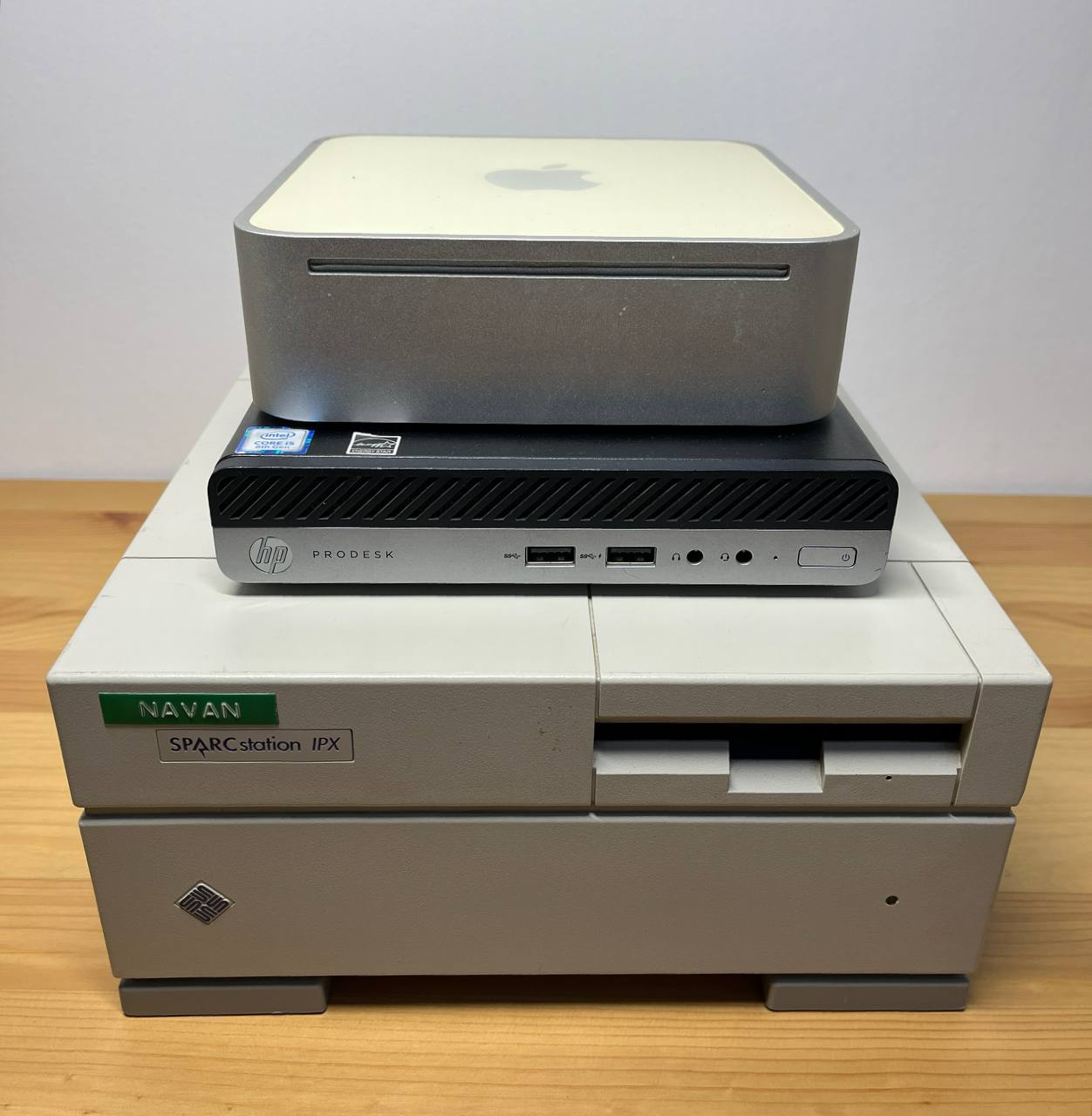
First things first: This is the first post of the year, halfway in the year. A move got in the way but a few fun things are in the pipeline :) With that out of the way, let’s take a peek in how small computing could be in the early 1990s. Nowadays small form factor computers are everywhere. Intel’s NUC from the early 2010’s, Apple launched the Mac Mini in the mid 2000s, and plenty more examples exist. Most big brands make tiny computers for office use that just take up 1L of space. But back in the late 80s and early 90s, this was not that common. One of the earlier tiny computers was the Sun SPARCstation IPC, and a little later the Sun SPARCstation IPX. At roughly 26x26x13cm it’s not small by modern standards, but back in the day it sure was tiny!
It’s not the smallest but at least the IPX has the power supply internally!
The Sun SPARCstation IPX in this photo was send to me by a friend to repair, as it didn’t output anything on a monitor. So let’s have a peek inside, see how to repair it and take a look at what kind of maintenance a computer from 1991 needs!
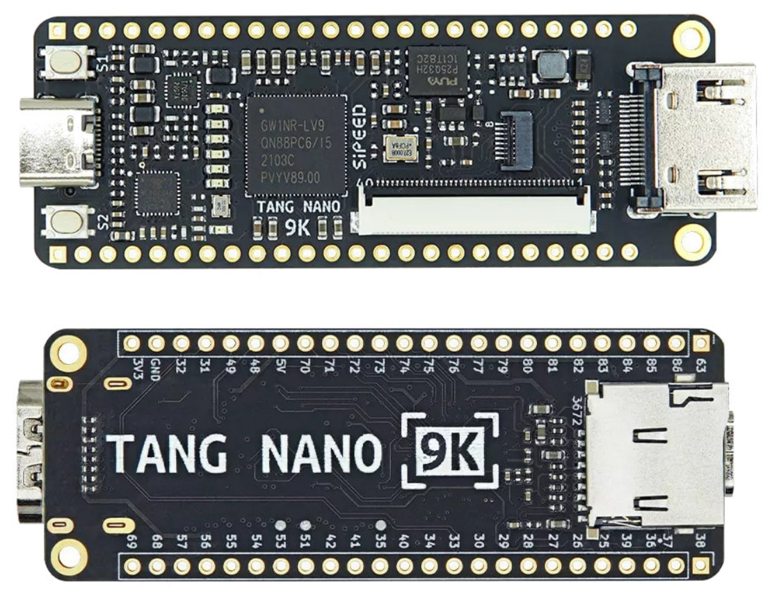
I always liked the idea of Litex, a framework to easily build a SoC for an FPGA, but never really made time to try it out. So let’s change that and write down how it went! I am using a Sipeed Tang Nano 9K FPGA board, which is a fairly cheap bit of kit, but most of this blog should apply to any supported FPGA.
Now, there was a little bit of a learning curve. Litex is written in Python, or a little more specific, it uses Migen, a python based tool that generated Verilog. I never coded much Python, let alone Migen. I wanted to learn a couple of things to say I know the basics of Litex
Understand a minimal SoC example
Customize a SoC with some peripherals already in Lite
Code custom firmware and run it on the created SoC
Have a way of working that’s somewhat pleasant to use
Before I get to all of that, let’s first install Litex and build an example!
Building the example SoC
If running a modern Linux, this is fairly straightforward, and following their guide works on Debian 12. To be able to build some examples, the standard or full config is needed, and a RISC-V toolchain needs to be installed. Luckily the quick start guide nicely explains all that and how to do so.
Now to the Gowin toolchain. It’s not open source, but free at least, but you need to apply for a free license. It can be downloaded here after registering. An open source toolchain is being developed but at the time of writing not complete enough to use with Litex.
The gw_sh binary from Gowin has to be added to the path, so a line in the likes of this in .bashrc should do:
PATH="$PATH:/path/to/gowin/IDE/bin"
After installation, navigate to the “litex/litex-boards/litex_boards/targets” folder and run:
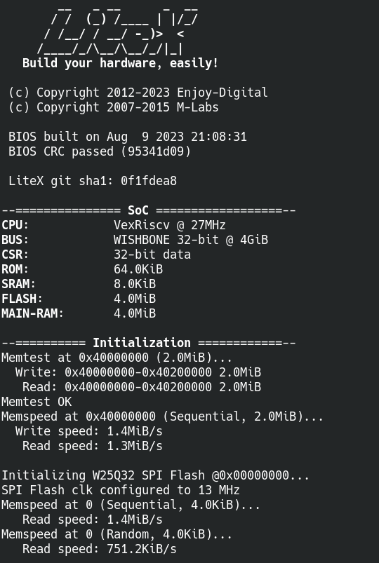
./sipeed_tang_nano_9k.py --build --flash
This will take a good bit of time, but it should compile, synthesize, PnR and then flash the fpga. The LEDs will blink in a nice pattern and when a serial port is opened at 115200 baud to the board, the following should greet you:
Pfff, that was a bit of work to get going, something to put in a docker perhaps…. :)
Now I can build the example, but I have no clue what it all does. Luckily a minimal example is included, let’s just take a peek at that. I took a moment to remove all that I could from the sipeed 9K example to more match the simple.py example and ended up with this:
import os
from migen import *

from litex.gen import *

from litex_boards.platforms import sipeed_tang_nano_9k

from litex.build.io import CRG
from litex.soc.integration.soc_core import *
from litex.soc.integration.soc import SoCRegion
from litex.soc.integration.builder import *

kB = 1024
mB = 1024*kB

# BaseSoC ------------------------------------------------------------------------------------------
class BaseSoC(SoCCore):
    def __init__(self, **kwargs):
        platform = sipeed_tang_nano_9k.Platform()

        sys_clk_freq = int(1e9/platform.default_clk_period)

        # CRG --------------------------------------------------------------------------------------
        self.crg = CRG(platform.request(platform.default_clk_name))

        # SoCCore ----------------------------------------------------------------------------------
        kwargs["integrated_rom_size"] = 64*kB
        kwargs["integrated_sram_size"] = 8*kB
        SoCCore.__init__(self, platform, sys_clk_freq, ident="Tiny LiteX SoC on Tang Nano 9K", **kwargs)

# Build --------------------------------------------------------------------------------------------
def main():
    from litex.build.parser import LiteXArgumentParser
    parser = LiteXArgumentParser(platform=sipeed_tang_nano_9K_platform.Platform, description="Tiny LiteX SoC on Tang Nano 9K.")
    parser.add_target_argument("--flash",                action="store_true",      help="Flash Bitstream.")
    args = parser.parse_args()

    soc = BaseSoC( **parser.soc_argdict)

    builder = Builder(soc, **parser.builder_argdict)
    if args.build:
        builder.build(**parser.toolchain_argdict)

    if args.load:
        prog = soc.platform.create_programmer("openfpgaloader")
        prog.load_bitstream(builder.get_bitstream_filename(mode="sram"))

    if args.flash:
        prog = soc.platform.create_programmer("openfpgaloader")
        prog.flash(0, builder.get_bitstream_filename(mode="flash", ext=".fs"))
        prog.flash(0, builder.get_bios_filename(), external=True)

if __name__ == "__main__":
    main()
Wow, that’s around 50 lines, not too bad. But it turns out, a lot of magic happens in Litex to keep this small. Let’s try to break it down a bit!
But what does it all do?
First, some imports and defines,
from litex_boards.platforms import sipeed_tang_nano_9k
imports the platform file, this file contains all the IOs and peripherals, it also includes some information about the programmer to use and the clock speed of the on board oscillator. For a custom board, a file like this has to be created from scratch.
The rest of the imports pull in migen, the HDL language used in Litex, and some basic builders to build the SoC.
import os
from migen import *

from litex.gen import *

from litex_boards.platforms import sipeed_tang_nano_9k

from litex.build.io import CRG
from litex.soc.integration.soc_core import *
from litex.soc.integration.soc import SoCRegion
from litex.soc.integration.builder import *

kB = 1024
mB = 1024*kB
Now time to jump to the bottom of the code and take a look at the main function:
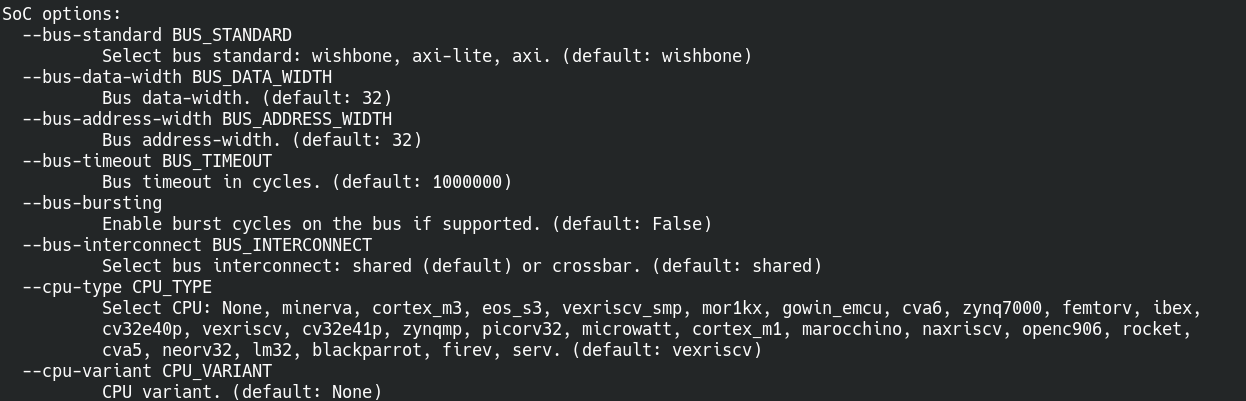
First of all, the LitexArgumentParser is imported and instantiated. This is a super handy feature in Litex that makes it easy to custimize a SoC with command line arguments. Run
./sipeed_tang_nano_9k.py --help
to get all the options, here is just a few of them for example:
Yes, selecting a different CPU is just a command line argument away, awesome!
Then the BaseSoc function is called, which is used to customize our SoC. We’ll look at that in a bit. Then the Litex Builder is called with our SoC as argument to generate the final SoC.
At last, the –load and –flash argument are handled. They both call the OpenFPGALoader tool to either load a bitstream in RAM or flash it in SPI flash on the FPGA board. The OpenFPGALoader tool is installed with the Litex_setup script.
The BaseSoC class creates the SoC to be fed into the Litex Builder in a bit. A basic SoC in Litex contains a Vexriscv CPU, wishbone bus, some RAM, ROM, a timer and a UART peripheral. But that’s the basics, it can be customized here. For now I specify the system clock frequency and generate a CRG. CRG means Clock Reset Generator and should contain any clocks and resets. For now there is just a single clock but let’s look into that more later on.
I also specify the rom and ram size, but this could even be removed if the defaults are fine. All this information is fed into the SoCCore.__init__ function that returns our SoC.
And there we go, a minimal SoC, awesome. It can also be viewed in full in Github.
Now let’s slowly add some new functions to it!
Adding a clock reset generator
The CRG currently is very limited compared to the one in the example. There isn’t even a reset button! Let’s change that and introduce a PLL and a Reset.
Compared to before, the CRG now uses one of the user buttons as a reset input. A PLL is generated that for now has the same input frequency as output frequency, but this can be changed by passing a parameter with a requested system clock frequency, neat! The reset pin resets the PLL, which in term resets the CPU. A full diff compared to the previous SoC can be seen here.
Finally, peripheral time!
There are quite a few peripherals already available in Litex, timers, uart, I2C, SPI and more. Sadly the documentation can be a little lacking, but after some digging around I got most of them to work. So let’s add a few things in the sipeed_tang_nano_9k.py file!
To add some peripherals, first they need to be imported:
from litex.soc.cores.timer import *
from litex.soc.cores.gpio import *
from litex.soc.cores.bitbang import I2CMaster
from litex.soc.cores.spi import SPIMaster
from litex.soc.cores import uart
There, that takes care of the most common ones. Instantiating is luckily pretty easy too!
Two more timers, some LEDs, I2C, UART and a GPIO input, just in a few lines. That is a TON easier then doing this in VHDL or Verilog. Now the platform file needs to be expanded a bit too so Litex knows what to place on what IOs:
Perfect! But there is a small tiny issue still. Well two actually. But the first one that is bothering me is that editing this all in the litex-boards repo is not really, ideal.
Time to make a separate folder for all of this, heck, a docker would be even nicer.
Containerize it all
When talking with a friend about running this all on a macbook, and the gowin IDE being not available for Mac OS he whipped up a small docker container for setting it up, just enter a license file location and good to go! I made a few small changes to it, mostly to set the workdir and add vim. So checkout that repo and give it a go!
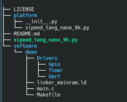
With this, it should be possible to run Litex with the Gowin tooling reliable on any computer, regardless of OS and distro. Ok, that is one issue taken care of, now to separate it all. I finally settled on a folder with the following structure:
platform contains the platform file and software the C source code for the program on the SoC, which can be found on my Github.
When starting the docker container, I bind the folder to docker as such:
The license file depends on mac address, so be sure to set your mac address in the docker to match the one for your license. Best would be to use a mac address generator and check that nothing in your network uses the generated mac address so there is no chance of any collisions or other network shenanigans.
After starting the container I end up in the correct folder immediately and I’m a single
./sipeed_tang_nano_9k.py --build
away from building!
Alright, the software folder is already showing up in there, but how did I get that far is another story.
Software woes
To start with, I looked at the demo application in Litex, and compiled that. It can be “uploaded” by integrating it in the internal rom of an SoC, but that means rebuilding the entire SoC on every software change. That’s quite hassle if you want to quickly reiterate on code.
Luckily, Litex also has a nice program called litex_term, which can be used to upload binaries and to have a terminal connected to the SoC. The default bios in Litex can accept a binary on boot, and run it, a little like the bootloader in an Arduino. Using it is pretty simple, run
litex_term /dev/TTYhere --kernel=yourapp.bin
and to upload the binary again after a change, just reset the board!
Now, this means there must be some RAM on your SoC that can be changed and is not used for the bios code. Can’t have your new code loaded in the RAM of the bios application of course. On some FPGA’s there is enough space to have 2 big blocks of RAM, but I opted to use the internal HyperRAM of the FPGA. This is also what the example uses and that seems to work quite well. The code to add this to the SoC is as follows:
        # HyperRAM ---------------------------------------------------------------------------------
        if not self.integrated_main_ram_size:
            # TODO: Use second 32Mbit PSRAM chip.
            dq      = platform.request("IO_psram_dq")
            rwds    = platform.request("IO_psram_rwds")
            reset_n = platform.request("O_psram_reset_n")
            cs_n    = platform.request("O_psram_cs_n")
            ck      = platform.request("O_psram_ck")
            ck_n    = platform.request("O_psram_ck_n")
            class HyperRAMPads:
                def __init__(self, n):
                    self.clk   = Signal()
                    self.rst_n = reset_n[n]
                    self.dq    = dq[8*n:8*(n+1)]
                    self.cs_n  = cs_n[n]
                    self.rwds  = rwds[n]
            # FIXME: Issue with upstream HyperRAM core, so the old one is checked in in the repo for now
            hyperram_pads = HyperRAMPads(0)
            self.comb += ck[0].eq(hyperram_pads.clk)
            self.comb += ck_n[0].eq(~hyperram_pads.clk)
            self.hyperram = HyperRAM(hyperram_pads)
            self.bus.add_slave("main_ram", slave=self.hyperram.bus, region=SoCRegion(origin=self.mem_map["main_ram"], size=4*mB))

        self.add_constant("CONFIG_MAIN_RAM_INIT") # This disables the memory test on the hyperram and saves some boottime
Now that is one hurdle, but I want to be able to compile my own code, separate from the litex repo’s, but while using their pre-made drivers and such. After some experimentation, I ended up with the following makefile. The magic bits are the build and include dirs at the top:
BUILD_DIR=../../build/sipeed_tang_nano_9k
SOC_DIR=/usr/local/share/litex/litex/litex/litex/soc/

include $(BUILD_DIR)/software/include/generated/variables.mak
include $(SOC_DIR)/software/common.mak
Oddly enough, in the readme for the demo, Litex uses a small python script to compile. I decided to just stick with a makefile as that is also what the python file seems to call. My code is very much based on the demo application, first stripped and then with new code for the new peripherals added.
Peripheral drivers
After generating an SoC with some IOs, I2C and more, I want to use those peripherals! Most of them are quite simple to use, but there is not really any documentation on how to do so. The best course of action is to look at the migen code and let Litex generate a document with all the registers. The can by done by adding the “–soc-csv” option. For example:
will output a file soc.csv with all the registers inside. –soc-json and –soc-svd are also possible for JSON and SVD files.
Some C include files are also generated on a build, especially csr.h in the build/sipeed_tang_nano_9k/software/include/generated/ is very useful, and for small peripherals using the functions in here is perfectly viable.
As an example, for reading the gpio pins, the “gpio_in_read” function works as expected.
For some, there are drivers available in Litex. I2C for example has a driver that works really well and can handle more then one I2C peripheral being generated, awesome!
One thing that was not clear however was using interrupts, so let’s take a dive into that real quick!
Interrupt woes
Enabling interrupts is pretty easy on the Litex/FPGA side of things. In general the irq.add function will take care of all that! For example:
I removed some #defines for clarity, but it will only handle the uart interrupt for the default uart! So either I need to change this file in Litex, or not use the Litex libraries. Ooooor make a small change and a PR. What I did is change the above code to the following:
// Weak function that can be overriden in own software for any IRQ that is not the uart.
// Return true (not zero) if an IRQ was handled, or 0 if not.
unsigned int __attribute__((weak)) isr_handler(int irqs);

// Override by default with return 0
unsigned int isr_handler(int irqs)
{
	return 0;
}

...

void isr(void)
{
	__attribute__((unused)) unsigned int irqs;
	irqs = irq_pending() & irq_getmask();
	if(irqs & (1 << UART_INTERRUPT))
		uart_isr();
	else
		if(!isr_handler(irqs))
			printf("Unhandled irq!\n");
}
So a simple __weak__ function is defined at the top, a weak function means that if the exact same function exists anywhere else, it will override the weak function. If it doesn’t exist it will call the weak function.
This means that if an interrupt happens that is not the uart interrupt, it will call the isr_handler(). If you implement it in your own code, awesome, it goes there and runs that. Otherwise no harm done, it will call the one in here.
In this case, if the interrupt that happens is the GPIO_INTERRUPT, I will handle it and return 1, otherwise 0 and the isr can throw a nice warning :) This is currently on a branch as a PR and not merged, so for now make sure to use that branch!
In the style of the original demo, I created a program with that reads the serial port and can execute a few commands to test I2C, gpio, timer interupts and so on. The full code can be found here. Now there is just one small thing left I’d like to figure out. Making my own peripheral!
Creating a custom peripheral
To get a bit of a feeling for making a peripheral, I decided to make a simple pwm peripheral. Something simple that just generates a PWM signal at a given frequency and duty cycle. Internally it should have a counter and when the counter is below or above a certain value toggle an IO pin to control the PWM duty cycle.
It should have a few registers:
An enable register, to enable/disable the PWM peripheral
A divider register, to be able to make lower frequency PWM signals
A maximum count register, it should count to this value and then reset it’s internal counter
A duty cycle register, if the counter is below this value, the IO pin should be low, otherwise it should be high.
That all sounds pretty doable, and while Migen reads quite different then Verilog or VHDL, it does make for some compact code because of all the Litex goodies.
For starters, making a register and connecting it to a CPU is very easy:
from migen import *

from litex.soc.interconnect.csr import *
from litex.gen import *

class PwmModule(LiteXModule):
    def __init__(self, pad, clock_domain="sys"):
        self.divider = CSRStorage(size=16, reset=0, description="Clock divider")
Just a few lines, and a simple peripheral is made! It just is a single 16 bits register but hey, that’s pretty amazing! No need to worry about CPU busses or anything. The CSRStorage is not the fastest method but for a peripheral like PWM it’s plenty.
So let’s quickly make that complete peripheral shall we!
A few more registers, and some internal counters for dividing the clock signal and the PWM counter. A complete and usable peripheral in a little over 30 lines, awesome!
And to use this peripheral in the SoC, just a single line is needed:
self.pwm0 = PwmModule(platform.request("pwm0"))
On the software side, just a few registers need to be set:
And with that all settled, the complete code for the SoC can be found here.
Conclusion
That was fun! From nothing to an FPGA SoC with some custom peripherals going on, awesome. And that in quite a small number of lines of code. I’m pretty amazed by what Litex can do!
Of course, it’s not perfect, and currently the at times lacking documentation is a bit of a bummer. Hopefully this blog at least helps a little. I am considering to look at creating some more advances peripherals, that HDMI port is alluring! I also want to at some time look at mixing Verilog/VHDL and Migen, which should be very possible. For now I think that this blog is long enough already.
If you enjoyed this blog, please consider buying me a coffee!
A long while back I picked up an old Tektronix logic analyzer. It was in decent shape but threw an error on the self test. To be more specific, the triggering board was faulty. But that means it was almost free and how can I say no to a repair job! Especially to some weird fun Tektronix box with a CRT touchscreen.
So let’s have a look inside and see what the issue might be.
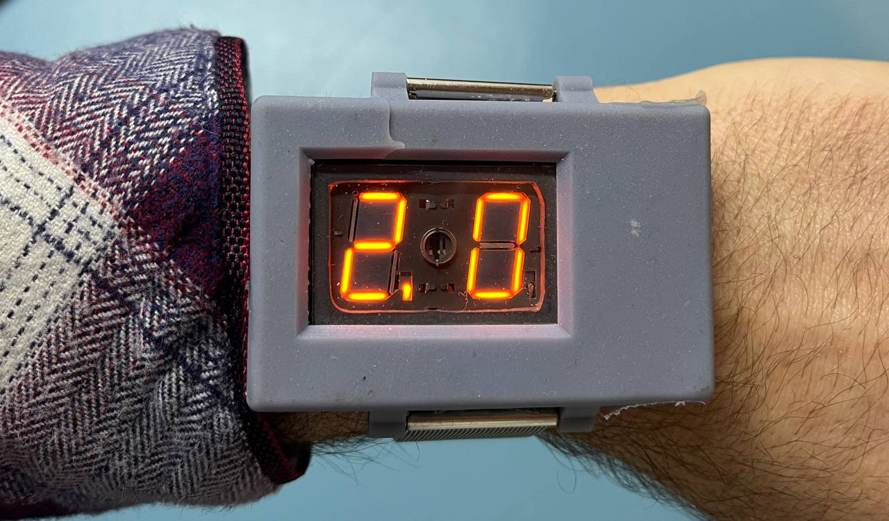
Ok ok ok, this is not a Nixie, it’s a Panaplex watch, but that sounds so much less fun. They work like nixies, but they are flat and often 7 segment displays, somewhat common in alarm clocks and tech gear.I got a few of them from a friend and compared to nixies, they are rather small and flat. So why not make a wristwatch with them!
Like nixies, panaplex displays require a high voltage to operate, around 200V. Which, on a wristwatch is a little challenging. I also wanted this to be a somewhat usable watch, unlike some of the nixie watches that, while cool, look quite cumbersome to wear due to their size.
This display is the ZM1570, which according to the datasheet, is similar to the ZM1550 but a little radioactive, fun!
So let’s look at what it takes to make a watch with these and how small all the circuitry can be.
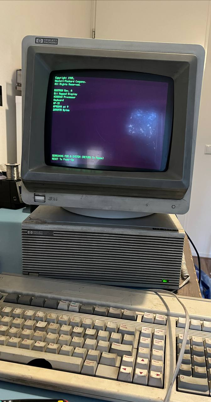
Yes I bought more 1980s computers. This time an HP9000/310. This is a computer launched in 1985 meant to control measuring equipment via HPIB, the interface later renamed to GBIP and still in use today. Now, a computer from the 80s meant to control EE equipment is not something I could not buy right?
The computer was stored working, but a little dirty. I first checked if the power supply was operating in spec and if there was any visible damage from things like leaking capacitors or batteries. That all seemed OK, so let’s turn it on!
And indeed, it still works! Now let’s take a good look at it, give it a clean and see if I can make it do something fun.