
I like CPU architectures, especially weird, interesting and unusual ones. For example, the Intel iAPX 432 is still something I would love to play around with. Recently, I realized that a working CPU can be made with just a simple Move instruction. For this to work, everything needs to be memory mapped. The ALU, program counter, everything.
Of course, this idea is nothing new and this idea is called the Transport Triggered Architecture. I decided to have a look into this, how it works and make a simple TTA CPU.
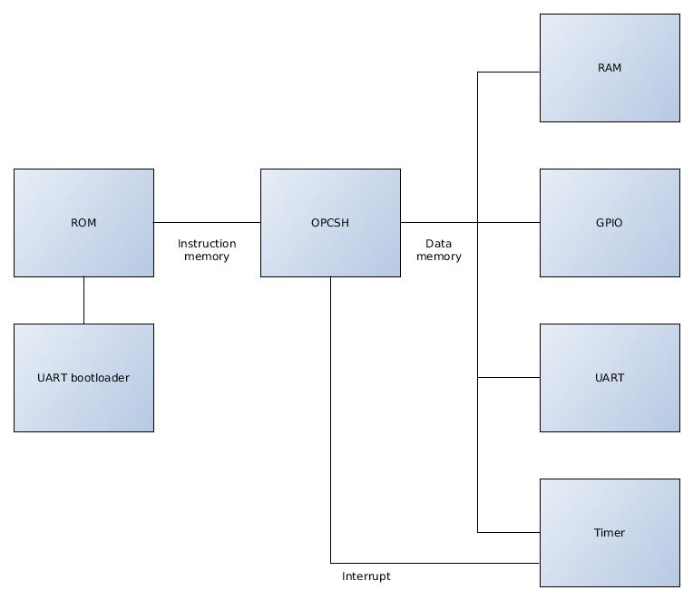
How does a TTA CPU work
Before I can make a CPU, let’s look into what is so different in a TTA CPU. In most CPU’s, calculations are done using registers and some arithmetic logic unit. For example, to add 2 numbers, the assembly code could be:
LOAD VARIABLE1, REGISTER0
LOAD VARIABLE2, REGISTER1
ADD REGISTER0, REGISTER1, REGISTER2
STORE REGISTER2, VARIABLE3
In a TTA CPU, there is no ALU or registers in the CPU itself. Instead, they exist somewhere in memory. In order to add 2 numbers, they are moved from memory or registers, to the ALU. The ALU result is then moved back to memory/registers. Or in code:
MOVE VARIABLE1,  ALU_A
MOVE VARIABLE2,  ALU_B
MOVE ALU_ADD_RESULT, VARIABLE3
In the simplest form, the CPU in a TTA CPU only needs to move data from one memory address to another. All calculations are done as a result of data being moved around. If you think, how would you jump to a different section of code, it’s easy. If the program counter is also in memory, a jump is as simple as moving a new address to the program counter.
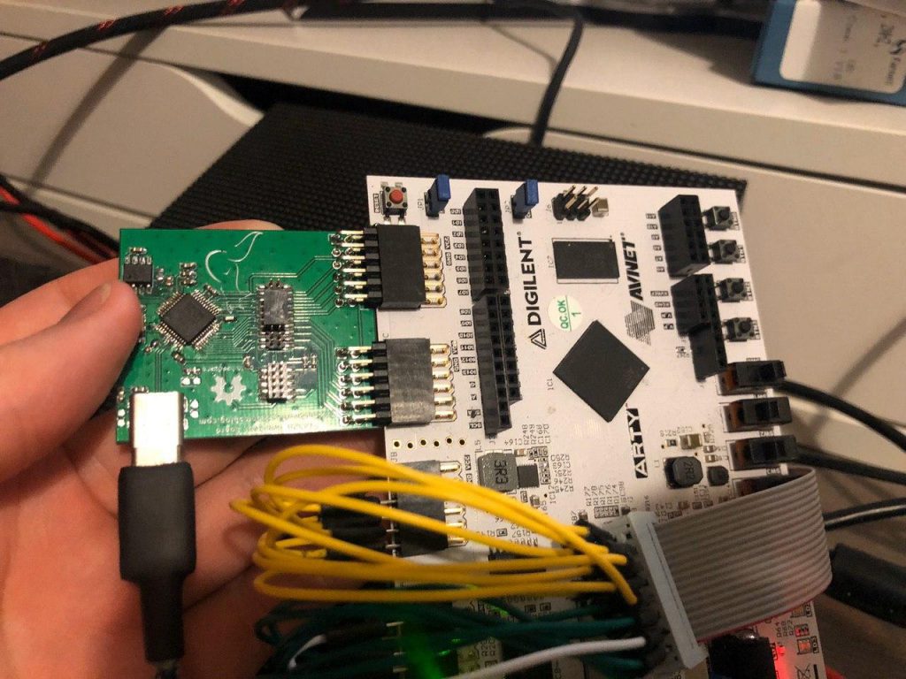
A few TTA computers have been made, and even commercially sold. But in general, it’s a niche architecture that never has gotten popular. So let’s build one :D
Continue Reading